
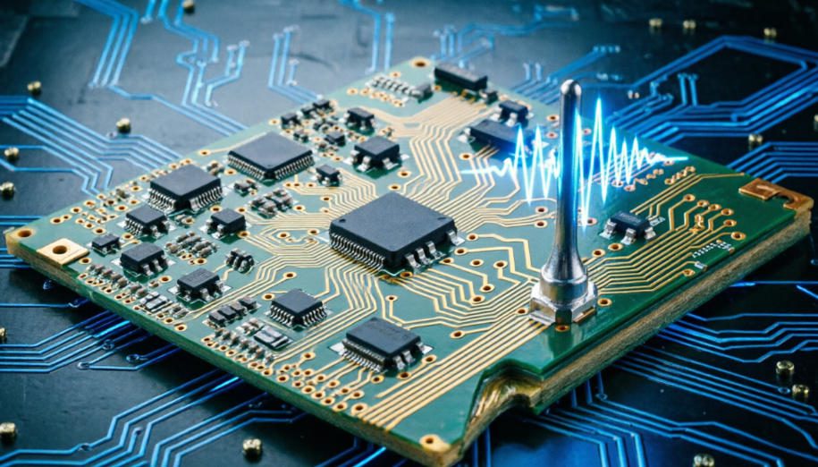
RF PCB Decoded: Design, Materials, and Industry Applications
When engineers ask, “what is RF PCB?“ they are typically looking for a circuit board designed to handle high-frequency signals, generally operating above 100 MHz. Unlike standard digital PCBs, these boards require specialized materials and layout techniques to manage impedance and minimize signal loss. Understanding what is RF PCB technology is crucial for ensuring signal integrity in modern wireless communications. This guide breaks down the core principles, material science, and real-world implementations.
Why Do RF Circuits Need Special Materials?
The Physics of High-Frequency Signals
At high frequencies, electrical signals behave more like waves than simple currents. Standard FR4 materials, commonly used in consumer electronics, become lossy and unstable. The dielectric constant (Dk) and dissipation factor (Df) of the substrate must be tightly controlled to prevent signal degradation.
Material Selection Criteria
Choosing the right laminate is the first step in successful RF design. Materials are selected based on:
- Thermal Stability: How the Dk changes with temperature.
- Moisture Absorption: Water ingress changes electrical properties.
- Z-axis Expansion: Critical for via reliability during thermal cycling.
How Is an RF PCB Different from a Standard PCB?
Signal Integrity vs. Connectivity
While a standard PCB focuses on connecting components electrically, an RF PCB focuses on signal integrity. The physical geometry of the traces acts as a transmission line (such as Microstrip or Stripline).
| Feature | Standard PCB | RF PCB |
|---|---|---|
| Primary Goal | Electrical Connectivity | Signal Integrity / Waveguide |
| Trace Geometry | Width based on current | Width based on Impedance |
| Reference Plane | Can have splits/gaps | Must be solid, continuous plane |
How Do You Design the Stack-up?
The Importance of Layering
A poor stack-up can ruin an RF design regardless of how good the layout is. The goal is to provide a consistent return path for signals and to isolate noisy digital sections from sensitive analog sections.
Best Practices for Layer Arrangement
- Adjacent Ground Plane: Place a solid ground plane directly under the RF trace. This minimizes loop area and reduces EMI.
- Minimize Dielectric Thickness: Keep the distance between the RF trace and the ground plane small to increase capacitance and reduce inductance.
- Isolate Digital Noise: If the board is mixed-signal (RF + Digital), place a power plane or ground plane between the layers to act as a shield.
What Are the Top Routing Challenges?
Impedance Control is Mandatory
RF traces must be routed with specific widths to match the system impedance (usually 50Ω or 75Ω). This is calculated using the trace width, thickness, and the dielectric constant of the material.
Avoiding Parasitics
Parasitic capacitance and inductance become significant at high frequencies. Avoid sharp bends (use curved or 45° mitred corners instead of 90° angles) and minimize the number of vias, as each via adds inductance.
How Do You Isolate RF and Digital Sections?
The “Moat” Strategy
Digital circuits generate noise that can couple into sensitive RF receivers, causing desense or blocking. A common technique is to create a “moat” (a gap in the copper) between the digital and RF sections on all layers.
Strategic Component Placement
- Group by Function: Place all RF components (amplifiers, filters, antennas) close together in one physical area.
- Guard Rings: Use grounded vias around sensitive traces to act as a Faraday cage, preventing radiation leakage.
What Manufacturing Tolerances Matter?
Precision in Production
RF performance is highly dependent on the physical dimensions of the board. Manufacturing variations can shift the center frequency of a circuit.
- Etching Tolerances: Even slight over-etching or under-etching changes trace width, altering impedance.
- Drilling Accuracy: Misaligned vias can change the capacitance in the transmission path.
Which Industries Rely on RF PCBs?
1. Telecommunications
In 5G base stations and small cells, RF PCBs handle massive data throughput. High-frequency laminates are essential here to maintain signal strength over long distances without overheating.
2. Aerospace and Defense
Radar systems and satellite communications require extreme reliability. These applications often use multi-layer boards with embedded passives to fit complex circuitry into tight spaces.
3. Medical Electronics
Devices like MRI machines and wireless patient monitors use RF PCBs for data transmission. The focus here is on biocompatibility of materials and zero signal loss to ensure patient safety.
4. Automotive (ADAS)
Modern driver-assistance systems (ADAS), such as collision avoidance radars, rely on 77GHz RF sensors. These boards must withstand extreme temperature fluctuations under the hood.
Frequently Asked Questions (FAQ)
What is the standard impedance for an RF PCB?
The most common characteristic impedance is 50Ω, chosen as a good compromise between power handling and low loss. However, video transmission often uses 75Ω.
Can I use FR4 for RF designs?
You can use FR4 for frequencies below 2 GHz if cost is the primary driver. However, expect higher signal loss and sensitivity to temperature changes compared to PTFE or ceramic-based laminates.
Why is the ground plane so important?
The ground plane provides the return path for the signal. Without a solid, low-impedance return path, the signal loop area increases, turning the PCB into an unintended antenna that radiates noise.
What is the “Skin Effect”?
As frequency increases, electrons tend to flow on the surface of the conductor rather than through its core. This reduces the effective cross-sectional area of the trace, increasing resistance and generating more heat.
Ready to turn your RF design into a reality? We understand that high-frequency projects require precision and flexibility. Thindry offers on-demand customization to meet your exact specifications, ensuring your board performs exactly as simulated. To help you optimize your design before production, we also provide free DFM (Design for Manufacturability) reports. If you need a quote or technical support for your next what is RF PCB project, contact us at sales@pcbtry.com.
0 Comments