
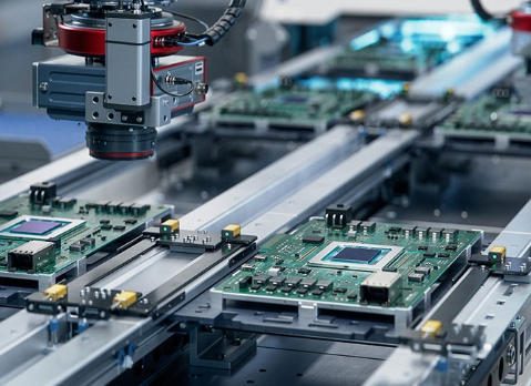
A PCB place refers to the precise positioning and arrangement of electronic components on a printed circuit board (PCB) during the design and manufacturing process. The goal of a PCB place is to ensure optimal signal integrity, thermal management, and manufacturability, while maximizing space efficiency. This guide breaks down everything you need to know about PCB place, including common pain points, industry applications, and best practices to get it right the first time.
What Is PCB Place, and Why Does It Matter for Electronic Devices?
A PCB place is the strategic layout of components—such as resistors, capacitors, ICs, and connectors—on a PCB. It is not just random placement; it directly impacts a device’s performance, reliability, and production yield.
Poor PCB place leads to signal interference, overheating, manufacturing defects, and even device failure. Proper PCB place ensures components work together seamlessly, reduces production costs, and extends the device’s lifespan.
How to Do PCB Place Correctly? Step-by-Step Best Practices
What Are the First Steps in PCB Place?
Start by defining the PCB’s size, shape, and layer stack-up. Next, identify critical components (e.g., power regulators, high-frequency ICs) and place them first to prioritize their performance needs.
Always follow datasheet guidelines for component spacing and orientation—this avoids issues like soldering defects or signal degradation later.
What Are the Key Rules for Component Spacing in PCB Place?
Component spacing is non-negotiable for manufacturability and performance. For surface-mount devices (SMD), keep same-type components at least 0.3mm apart.
For mixed SMD and through-hole components, maintain a 1-3mm gap to prevent soldering issues. Hand-soldered components need a minimum 1.5mm spacing for accessibility.
What Are the Most Common PCB Place Mistakes to Avoid?
The top PCB place mistake is ignoring component orientation—placing parts like electrolytic capacitors or diodes backwards ruins functionality. Another common error is overcrowding components to save space.
Placing heat-generating components (e.g., power ICs) near heat-sensitive parts (e.g., capacitors) also causes failures. Always leave space for airflow and thermal management.
How Does PCB Place Differ Across Key Industries?
PCB place requirements vary by industry, as each has unique performance and environmental demands. Below are real-world cases from four high-demand sectors, showing how PCB place solves specific challenges.
Consumer Electronics: PCB Place for Compact Smartphones
In smartphones, PCB place focuses on miniaturization and signal integrity. A high-density PCB place for a flagship phone’s main board places the processor, memory, and antenna modules in tight quarters.
This PCB place minimizes signal interference between the 5G antenna and other components, ensuring fast connectivity while fitting into a slim design.
Automotive Electronics: PCB Place for Vehicle Control Modules
Automotive PCB place must withstand extreme temperatures (-40℃ to +85℃) and vibration. For a vehicle’s engine control unit (ECU), PCB place separates power components from sensitive sensor inputs.
This layout prevents electrical noise from affecting sensor data, ensuring the ECU reliably regulates engine performance. We support custom on-demand solutions + free DFM reports for automotive PCB place to meet strict industry standards.
Industrial Control: PCB Place for PLC Modules
Industrial PLCs require PCB place that resists electromagnetic interference (EMI) and mechanical stress. A PLC’s PCB place groups relay drivers and power supplies away from signal processing components.
This design ensures stable operation in factory environments with high EMI, reducing downtime for industrial machinery.
Medical Electronics: PCB Place for Portable Monitors
Medical device PCB place must meet IEC 60601 standards for reliability and safety. For a portable patient monitor, PCB place positions the battery management system near the power connector.
This layout ensures consistent power delivery to vital sign sensors, preventing data errors that could impact patient care.
PCB Place vs. PCB Layout: What’s the Difference?
| Aspect | PCB Place | PCB Layout |
|---|---|---|
| Definition | Positioning of components on the PCB | Routing of copper traces to connect components |
| Focus | Component location, spacing, orientation | Trace path, impedance control, signal flow |
| Priority | Comes first; sets the foundation for layout | Follows PCB place; optimizes connectivity |
| Impact | Affects manufacturability and signal integrity | Affects signal speed and EMI performance |
How to Fix Poor PCB Place That Causes Signal Interference?
Fix signal interference from poor PCB place by repositioning high-frequency components (e.g., oscillators) away from sensitive parts (e.g., analog sensors). Use ground planes to isolate noisy components.
Ensure signal traces are short and direct, and avoid crossing high-speed and low-speed traces. A well-executed PCB place minimizes loop areas, which reduces EMI.
What Tools Help with Accurate PCB Place?
Popular tools for PCB place include Altium Designer, KiCad, and CircuitMaker. These tools offer component libraries, 3D visualization, and DFM checks to ensure proper placement.
Look for tools with real-time spacing checks and thermal analysis—these features prevent common PCB place mistakes before manufacturing.
FAQ: Common PCB Place Questions Answered
Can PCB Place Affect Manufacturing Yield?
Yes, poor PCB place directly lowers manufacturing yield. Overcrowded components or incorrect spacing cause soldering defects like bridging or tombstoning, leading to rejected boards.
Following PCB place best practices reduces defects, increasing yield and lowering production costs.
Do I Need to Consider Thermal Management in PCB Place?
Absolutely. Thermal management is critical in PCB place. Heat-generating components (e.g., power LEDs, voltage regulators) must be placed away from heat-sensitive parts.
Leaving space around hot components or using heat sinks ensures proper airflow, preventing overheating and component failure.
What Is the Ideal PCB Place for High-Frequency Components?
High-frequency components (e.g., RF modules) should be placed close to the PCB edge, near connectors, to minimize trace length. Keep them away from analog components to avoid interference.
Use ground planes beneath high-frequency components to reduce signal loss and EMI.
How Does PCB Place Impact Repairability?
Poor PCB place makes repair difficult. Placing small components under larger ones (e.g., resistors under a display) requires removing the larger part to access the smaller one, increasing repair time and risk.
Leave clear access to commonly failed components in your PCB place to simplify repairs.
Is There a Standard for PCB Place Spacing?
While there’s no universal standard, IPC-A-610 provides guidelines for component spacing based on component type and manufacturing process. Follow your manufacturer’s DFM requirements for optimal results.
For most SMD components, a 0.3mm minimum spacing is recommended, while through-hole components may require 1mm or more.
Can PCB Place Be Adjusted After Design?
Yes, PCB place can be adjusted after design, but it’s best to get it right initially. Adjustments may require rerouting traces, which can increase design time and cost.
Using DFM checks during the design phase helps avoid the need for post-design PCB place adjustments.
How to Ensure PCB Place Meets Industry-Specific Requirements?
Start by researching industry standards (e.g., IEC 60601 for medical, ISO 26262 for automotive). Work with a manufacturer that understands your industry’s needs.
We specialize in industry-specific PCB place, with experience in consumer electronics, automotive, industrial control, and medical devices. We support custom on-demand solutions + free DFM reports to ensure your PCB place meets all requirements.
Why Choose Thindry for Your PCB Place Needs?
At Thindry, we have years of experience in optimizing PCB place for all major industries. Our team of engineers ensures your PCB place is designed for performance, manufacturability, and reliability.
We provide PCB place services, including custom design and DFM analysis. If you need high-quality PCB place solutions, contact us to place your order at sales@pcbtry.com. We support custom on-demand solutions + free DFM reports to help you get the perfect PCB place for your project.


0 Comments