
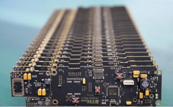
Main PCB assembly is the key process that integrates critical functional modules onto the main PCB of an electronic product. The main PCB acts as the system’s “central nervous system,” connecting microcontrollers, power modules, interface connectors, and other components to form a fully operational system. Without reliable assembly, even the most advanced chips and components cannot perform at their full potential.
Main PCB assembly directly impacts product performance, system stability, and manufacturing cost. High-quality assembly ensures signal integrity, stable power distribution, and long-term reliability. For example, in smartphones, it enables high-speed coordination between the processor, memory, and sensors; in industrial control devices, it ensures stable operation under high temperatures, vibrations, or electromagnetic interference.
This guide is intended for engineers, product designers, procurement specialists, and beginners interested in electronics manufacturing. It provides insights into the core value, key considerations, and practical guidance for main PCB assembly, helping to achieve efficient design and reliable production.
What is the main PCB assembly?
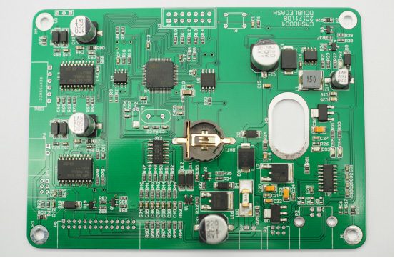
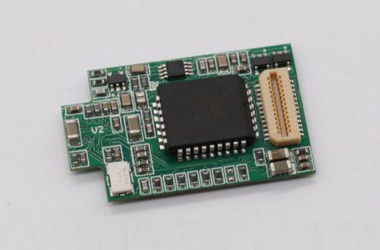
Main PCB assembly refers to the process of precisely mounting and soldering various electronic components onto the main printed circuit board (PCB) of a device. Unlike PCB fabrication, which only manufactures bare boards, PCB assembly introduces microchips, passive components, power modules, and interface devices, giving the circuit board true computing, control, and communication capabilities.
As the “core hub” of the entire system, the main PCB bears the critical responsibility of power distribution, signal transmission, and functional coordination. Its assembly quality directly determines the performance stability, system reliability, and long-term lifespan of the electronic product. Any design or assembly deviation can lead to signal interference, abnormal power consumption, or even complete system failure.
Key Components in Main PCB Assembly
A fully functional main PCB is typically composed of several core components working together, including:
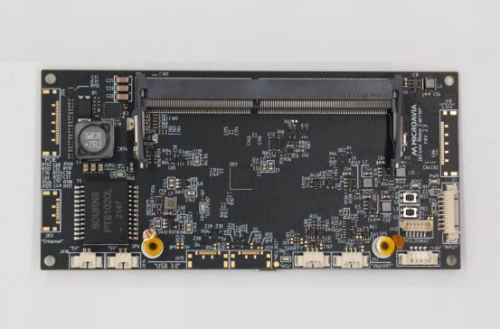
Microcontroller (MCU) or processor (CPU): Acting as the system’s “brain,” responsible for data processing, logic operations, and peripheral control;
Power management circuitry (PMU/PMIC): Providing voltage regulation, power distribution, and protection to ensure safe system operation under various conditions;
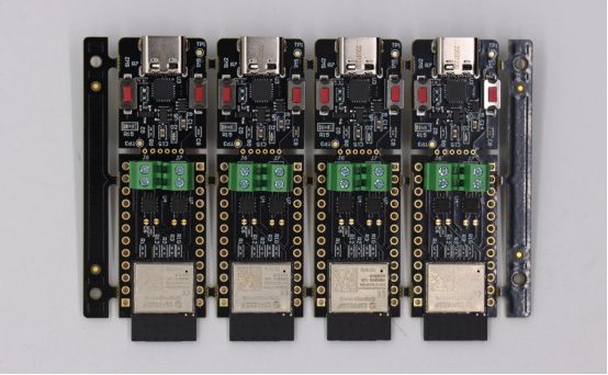
Connectors and interface modules: Such as USB, HDMI, header pins, or high-speed interfaces, used for communication with external devices or submodules;
Passive components (resistors, capacitors, inductors): Used for filtering, voltage regulation, impedance matching, and noise suppression to ensure signal and power stability.
These components collectively form the functional foundation of the main PCB, making it not just a circuit board, but the core platform supporting the operation of the entire system.
How to choose components and layouts?
In main PCB assembly, the selection and layout of components directly determine the upper limit of the circuit board’s performance. In low-frequency applications, as long as the components are functionally matched and correctly connected, the design is relatively flexible. However, in high-frequency, high-speed, or high-power scenarios, even minor layout deviations or improper component selection can lead to problems such as decreased signal integrity, increased crosstalk, or thermal runaway.
Therefore, the component layout of the main PCB must revolve around principles such as minimizing signal paths, power loops, and reasonable heat dissipation. Critical components (such as processors, high-speed interface chips, and power management ICs) should be placed close to their service targets to shorten signal loops and reduce the risks associated with impedance discontinuities. A reasonable component arrangement not only helps improve system stability but also reduces PCB size while meeting functional requirements, creating conditions for miniaturized product design.
Component selection is also one of the key decisions in the product development lifecycle. Engineers need to focus not only on the electrical performance and reliability of components but also on supply cycles, lifecycle status, and alternative solutions. In mass-produced products, selecting components with stable supply and high substitutability helps reduce supply chain risks and avoid production delays caused by shutdowns or delivery fluctuations. Only by taking manufacturability and sustainable supply into account during the design phase can the main PCB assembly achieve the best balance between performance and cost.
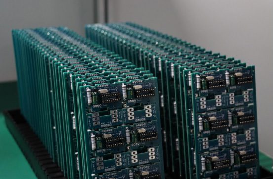
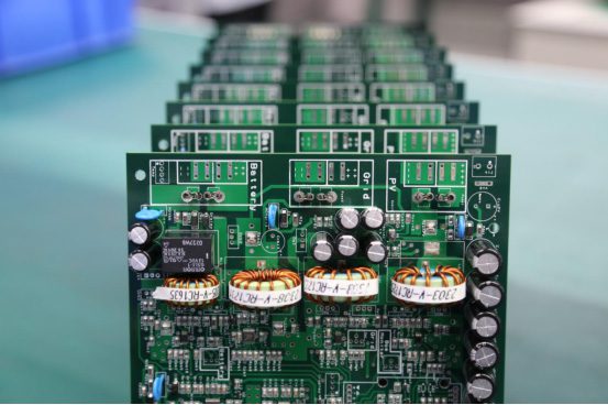
Main PCB Assembly Process
The core goal of main PCB assembly is to transform a bare board into a fully functional and reliable “motherboard.” This process typically consists of several highly standardized and interconnected steps, each directly impacting the quality and yield of the final product.
- PCB Design and BOM
The assembly process begins with PCB layout design. Engineers need to comprehensively consider signal integrity, power distribution, and heat dissipation paths during the design phase. Properly planning trace widths, pad sizes, and component spacing lays the foundation for subsequent automated assembly and stable operation.
Then, a BOM is generated, a crucial document connecting design and production. An accurate and traceable BOM effectively avoids rework and delays caused by incorrect part numbers or unavailable components, while also contributing to cost control and efficient procurement.
- Solder Paste Printing
Before component mounting, solder paste must be precisely printed onto the PCB pads using a stencil. Controlling the amount of solder paste used is critical: too much can cause solder bridging, while too little can lead to cold solder joints or open circuits. Stable and uniform solder paste printing is fundamental to improving overall assembly yield.
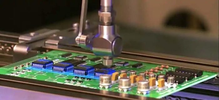
- Pick & Place
Automatic pick-and-place machines, based on coordinate information in the design files, place components quickly and precisely onto the solder paste locations. This step not only determines assembly efficiency but also directly impacts the success rate of subsequent soldering, making it one of the most precision-critical steps in main PCB assembly.
- Soldering and Fixing
After component placement, electrical and mechanical connections are achieved through soldering processes. Depending on component type and design requirements, common methods include reflow soldering (SMT), wave soldering (through-hole), and selective soldering (hybrid processes). Appropriate selection of soldering methods can ensure soldering quality while avoiding thermal damage to sensitive components.
What are the functions of the main PCB in an application?
In various electronic products, the main PCB plays a crucial role in system-level integration and control. Its design and assembly quality directly determine the overall performance and reliability of the device.
- Smartphones and Consumer Electronics
The main PCB connects the processor, memory, power management chip, and wireless communication module, serving as the core carrier for high-speed data exchange and multitasking. Proper layout and assembly effectively ensure signal integrity and energy efficiency.
- Industrial Control Equipment
In systems such as PLCs and industrial controllers, the main PCB coordinates sensors, relays, and actuators to ensure stable operation of the equipment under vibration, temperature differences, and electromagnetic interference, forming the foundation for automated control.
- Internet of Things (IoT) Terminals
The main PCB highly integrates the microcontroller, communication module (Wi-Fi/Bluetooth/cellular), and power system within a limited space, balancing size, power consumption, and performance while providing reliable long-term operation for terminal devices.
Common challenges and solutions
Even with a well-designed main PCB, quality and reliability risks may still exist during assembly. Identifying problems early and taking targeted measures is key to improving yield and reducing rework costs.
- Soldering Defects
Soldering issues directly affect the reliability of electrical connections. Common defects include:
Tombstone Effect:Caused by uneven solder paste or temperature imbalance, this can be improved by optimizing the stencil design and reflow profile.
Solder Bridging:Often caused by excessive solder paste or stencil misalignment. Solder paste thickness needs to be controlled and pad spacing optimized.
Cold Solder Joints:Usually caused by insufficient heating or surface contamination. Cleaning should be intensified and soldering temperature calibrated.
- Component Misalignment
Insufficient placement accuracy or transport vibration can easily cause component misalignment. Utilizing a vision alignment system, regular equipment maintenance, and optimizing board fixation can effectively improve placement accuracy.
- Thermal Management Issues
Poor heat dissipation can lead to performance degradation and even component failure. Common measures include adding thermal vias, using heat sinks or thermal pads, and widening power traces to ensure long-term stable operation of the main PCB.
Key differences between flexible and rigid PCB assembly
| Comparison Dimensions: | Rigid PCB Assembly | Flexible PCB Assembly |
| Substrate Material | FR-4, CEM series | PI, PET |
| Mechanical Properties | Non-flexible | Bendable, foldable |
| Structural Stability | Very high | Requires additional reinforcement |
| Design Flexibility | Primarily planar layout | Supports three-dimensional structures |
| Production Cost | Lower | Higher cost |
| Suitability for use as a motherboard | Very suitable | Typically not used as a mainboard |
| Batch Consistency | High | Relatively complex |
How to ensure the cleanliness of PCBA?
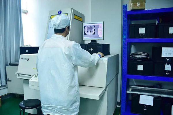
In the PCB assembly process, quality inspection is a critical step in ensuring the stable operation of the main PCB. Solder paste inspection typically involves measuring pad height and coverage using 3D SPI tools, while AOI (Automated Optical Inspection) is used to identify missing, incorrect, and misaligned components. X-ray inspection can detect internal defects in hidden solder joints such as BGAs. These systems can inspect critical solder joints at high speed, providing data support for process optimization.
After inspection, in-circuit testing (ICT) and functional testing are used to verify that the electrical performance meets design requirements. By combining AOI and X-ray data, the engineering team can continuously improve process stability and reduce defect rates through Statistical Process Control (SPC).
After successful inspection, professional cleaning of the PCBA effectively removes flux residue and contaminants, preventing corrosion, leakage, and other long-term reliability issues, thus extending product lifespan.
A comprehensive inspection system and standardized cleaning procedures are indispensable parts of high-reliability main PCB assembly.
Why choose us for PCB assembly?
Thindry is a leading one-stop service provider for PCB assembly in China, covering the entire process from PCB design and manufacturing to material procurement and assembly. Through efficient process management, we help customers reduce costs and shorten delivery times.
Extensive Industry Experience Ensures Quality Delivery
With over 20 years of experience in PCB and SMT assembly, Thindry can flexibly support diverse needs, from small-batch samples to large-scale mass production. Every project is strictly controlled by our experienced engineering team.
Advanced Systems and Equipment Ensure Stability and Reliability
Leveraging intelligent management systems such as CRM, MES, ERP, and IoT, and combining them with detection methods such as SMT defect detection and ESD electrostatic protection, we ensure that the quality of every PCB assembly is stable and traceable.
Authoritative Certifications Guarantee Quality
Having obtained multiple international certifications including ISO9001, IATF16949, and ISO13485, we strictly adhere to quality standards, making us a trustworthy PCB assembly partner.
Efficient Response and Professional Support
We provide fast and professional customer service, promptly responding to PCB assembly inquiries and quotation requests, facilitating efficient project progress.
FAQ
What does PCB stand for?
PCB stands for Printed Circuit Board, which is used to support and connect electronic components, allowing current to flow smoothly between components and ensuring the device functions properly.
Why do electronic devices need a main PCB board?
The main PCB board is the core framework of the device, carrying key components and transmitting signals and power between chips, sensors, and other components.
How many layers can a PCB board have at most?
PCBs can be single-layer, double-layer, or multi-layer. Simple devices typically use single-layer boards, while complex devices (such as computers) usually use multi-layer boards with four or more layers.
What materials do engineers use to manufacture PCBs?
Most PCBs use FR-4 fiberglass material. Some PCBs for high-temperature or special applications use plastic or ceramic. Copper layers are responsible for current transmission.
How do engineers test whether a PCB is working properly?
Engineers use methods such as AOI (Automatic Optical Inspection), X-ray, and electrical testing to check for open circuits, poor solder joints, and other problems to ensure that each PCB meets quality standards.


0 Comments