
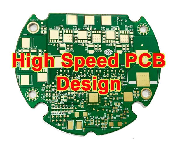
In today’s tech-driven world, High Speed PCB Design is the backbone of 5G devices, automotive ADAS, data centers, and IoT sensors. Whether you’re working with 100MHz signals or 28GHz mmWave technology, mastering High Speed PCB Design is critical to avoiding costly reworks, meeting industry standards, and delivering products that perform. This guide distills decades of engineering expertise into actionable steps, mistake-proofing strategies, and pro tips to simplify complex high speed design challenges.
What Is High Speed PCB Design? Key Definitions & Thresholds
Core Definition & Critical Speed Benchmarks
High Speed PCB Design refers to PCB layouts where signals travel at frequencies >100MHz or propagation times <1ns. At these speeds, signals act as electromagnetic waves, making signal integrity (SI), power integrity (PI), and EMC compliance non-negotiable. Unlike standard PCB design (focused on basic connectivity), high speed PCB layout demands precise control over impedance, trace routing, and layer stackups to prevent signal degradation.
Industry Standards for High Speed PCB Design
Reliable High Speed PCB Design requires adherence to IPC standards: IPC-2221 (design requirements for trace width, spacing, and hole sizes) and IPC-6012 (fabrication quality for rigid PCBs). These standards ensure consistency in material selection, copper thickness, and impedance control—critical for industries like aerospace, automotive, and telecommunications.
Why High Speed PCB Design Matters for Modern Electronics
Powering Next-Generation Technologies
High Speed PCB Design enables breakthroughs in 5G, automotive ADAS, and cloud computing. 5G base stations rely on high frequency PCB design to handle 28GHz signals with minimal attenuation, while automotive systems need real-time data transfer between sensors and ECUs. Without optimized high speed design, these technologies suffer from latency, signal loss, and frequent failures.
Cost Risks of Poor High Speed Design
Cutting corners in High Speed PCB Design leads to expensive reworks, delayed time-to-market, and regulatory fines. Poor signal integrity causes product failures during testing, while non-compliant designs risk recalls. Investing in proper high speed PCB layout upfront reduces long-term costs and ensures consistent performance.
Critical Factors Affecting High Speed PCB Performance
Signal Integrity (SI) – The Foundation of Reliability
SI is make-or-break for signal integrity PCB and High Speed PCB Design, covering reflections (impedance mismatches), crosstalk (unwanted signal coupling), and attenuation (signal loss over distance). These issues worsen at frequencies >1GHz, especially with standard FR4 material. Mitigation requires careful routing, impedance control, and material selection.
Power Integrity (PI) & Thermal Management
PI ensures components receive stable voltage—critical for High Speed PCB Design. Voltage noise in power delivery networks (PDNs) corrupts high-speed signals, so proper decoupling capacitor placement and plane design are essential. Thermal management (thermal vias, high-conductivity laminates) prevents overheating in high-frequency components.
Material Selection – Rogers vs. FR4
FR4 works for frequencies ≤1GHz but has high dielectric loss (Df) at higher speeds. For 2GHz+ applications (5G/RF), Rogers materials (e.g., RO4350B, Df=0.0037) minimize attenuation. Balance cost: FR4 suffices for consumer electronics, while Rogers is ideal for industrial/aerospace high frequency PCB design.
Step-by-Step High Speed PCB Layout Best Practices
Floorplan Optimization
Start with functional grouping: separate analog/digital circuits to avoid noise. Place critical components (crystals, ICs) near the board center to minimize trace lengths. Isolate high-speed paths from power traces and noisy components (e.g., DC-DC converters) for High Speed PCB Design success.
Component Placement & Via Management
Place ICs close to power sources and decoupling capacitors (≤50mil) to reduce PDN noise. Use blind/buried vias for 10Gbps+ signals to avoid stubs; backdrill unused via barrels. Limit vias to 2 per high-speed signal (each adds 0.1–0.2dB insertion loss).
Differential Pair Routing
Maintain equal length (±5mil for DDR4) and 100Ω±10% impedance. Route pairs parallel with no stubs; use 45° jogs for length matching. For dense boards, use stripline routing (between ground planes) to reduce crosstalk in high speed PCB layout.
Impedance Control – Non-Negotiable for High Speed Design
Calculating Transmission Line Impedance
Impedance (Z0) depends on trace width, thickness, material, and stackup. Use calculators (Rogers/Cadence) to determine dimensions: 100Ω microstrip on FR4 (1.6mm) typically requires 5mil trace width. Mismatched impedance causes 90% of reflection issues in impedance controlled PCB design and High Speed PCB Design.
Tolerance & Discontinuity Avoidance
Maintain ±10% impedance tolerance with ±7μm trace width accuracy. Avoid line width changes, right-angle bends, and stubs >5mil—these create discontinuities. Use 45° bends and solder mask dams for via transitions.
How to Avoid High Speed PCB Design Common Mistakes
Prevent Impedance Mismatches & Reflections
Match trace impedance to components (50Ω for RF, 100Ω for differential pairs). Add termination resistors (series/parallel) and backdrill vias. Never route high-speed signals across plane splits—this breaks return paths in impedance controlled PCB design.
Fix Cross-Plane Routing & Ground Plane Errors
Ensure every high-speed signal has a continuous reference plane. Avoid ground “islands” and use star grounding for mixed-signal designs (single-point analog/digital ground connection) in High Speed PCB Design.
Correct Length Matching & Via Overuse
Follow DDR4/PCIe tolerance (≤5mil within pairs, ≤20mil between pairs). Limit high-speed signals to 2 vias max; use zero vias for 25Gbps+ signals.
High Speed PCB Routing Techniques for Signal Integrity
45° Bends vs. Right Angles
Right-angle bends cause impedance spikes and EMI—use 45° bends or arcs (critical for >5GHz). Keep traces short to reduce attenuation/crosstalk in signal integrity PCB and High Speed PCB Design.
2W/3W Rule & Guard Tracing
Use the 2W rule (spacing ≥2x trace width) for ≤1GHz (reduces crosstalk by 70%); 3W rule for >1GHz. Add grounded guard traces (every 300mil) between high-speed signals.
Minimize Stubs & Signal Loops
Eliminate stubs >5mil and keep signal loops small (reduces EMI/inductance). Route signal/return paths close together (e.g., differential pairs, microstrip with ground plane).
Power & Ground Plane Design for High Speed PCBs
Layer Stackup Optimization
4-layer stackup (Top→GND→Power→Bottom) is minimum for High Speed PCB Design. 6-layer boards add inner signal layers between ground planes for better crosstalk control. Use symmetric stackups to prevent warping.
Decoupling Capacitors & Plane Capacitance
Place 0.1μF/1μF/10μF capacitors near IC power pins. Leverage power/ground plane capacitance (10mm² pair = ~1nF) for high-frequency filtering.
Manufacturing Considerations for High Speed PCBs
Fabrication Tolerances & Material Compatibility
Ensure fabricators meet drill size (±0.1mm), copper thickness (±10%), and trace width (±7μm) specs. Rogers materials require specialized processing (plasma cleaning) for high speed PCB manufacturing and High Speed PCB Design.
Cost vs. Performance & Quality Control
Use blind/buried vias only for critical signals (balance cost/performance). Require impedance testing (TDR/TDT), SI verification (eye diagrams), and EMC testing to ensure compliance in high speed PCB manufacturing.
Top High Speed PCB Design Software Tools (2026)
Cadence Allegro
Gold standard for complex High Speed PCB Design—robust constraint management and SI/PI simulation. Used by 60% of Fortune 500 tech companies (steep learning curve).
Altium Designer & Keysight ADS
Altium: Real-time impedance checking, user-friendly for startups. Keysight ADS: Specialized for 5G/RF (up to 100GHz) with advanced EM simulation—ideal for high frequency PCB design.
FAQ: Common High Speed PCB Design Problems & Solutions
Q1: How to fix signal reflections?
A: Match impedance, add termination resistors, and backdrill vias. Simulate with SI tools to identify mismatches in High Speed PCB Design.
Q2: Best material for 24GHz PCBs?
A: Rogers RO4350B (low Df=0.0037) minimizes attenuation. FR4 works for cost-sensitive designs but needs shorter traces in high frequency PCB design.
Q3: How to reduce crosstalk?
A: Use 3W rule, orthogonal routing, guard traces, and stripline routing. Avoid parallel high-speed traces >100mil in signal integrity PCB projects.
Q4: Why do high speed PCBs fail EMC testing?
A: Board edge radiation (keep signals 3W from edges) and ground bounce. Fix with proper plane design and decoupling in High Speed PCB Design.
Q5: How to handle thermal issues?
A: Use thermal vias, high-conductivity laminates, and strategic component placement in high speed PCB manufacturing.
Q6: Maximum length mismatch for DDR4?
A: ≤5mil within pairs, ≤20mil between pairs—critical for high speed PCB layout success.
Ready to Elevate Your High Speed PCB Design? Partner With Experts
Don’t let signal integrity issues, compliance gaps, or costly reworks slow your project. Our team of High Speed PCB Design specialists has decades of experience delivering IPC-compliant, high-performance layouts for 5G, automotive, and industrial applications. We handle impedance controlled PCB design, SI/PI simulation, and high speed PCB manufacturing optimization—so you get reliable boards on time and on budget. Ready to start your project? Email us today at sales@pcbtry.com to discuss your requirements and get a custom quote. Let’s turn your design vision into reality.


0 Comments