
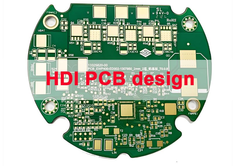
In the age of 5G, AI wearables, and compact industrial gear, HDI PCB design has emerged as the backbone of high-performance electronics. This advanced methodology—defined by microvias, blind/buried vias, and dense routing—solves the limitations of traditional PCBs, enabling smaller footprints and better signal integrity. Whether you’re engineering a smartphone motherboard or a high-speed server, mastering HDI PCB design is critical to delivering reliable, cost-effective products. Below, we share decades of industry expertise: actionable best practices, common pitfalls to avoid, and real-world insights that align with how manufacturers and engineers actually work.
1. What Is HDI PCB Design? Core Definitions & Key Traits
1.1 Essential Terms for Engineers
HDI PCB design (High-Density Interconnect PCB design) maximizes circuit density by using three key technologies: microvia design (laser-drilled holes as small as 0.075mm), blind vias (connect outer to inner layers without piercing the board), and buried vias (link inner layers exclusively). Via-in-pad technology—placing vias directly under components like BGAs—further reduces board size and signal path length.
1.2 Critical Specifications for Success
For manufacturable HDI PCB design, stick to these specs: minimum trace width/spacing of 3mil/3mil (0.075mm/0.075mm) for mass production, layer counts from 6-20+, and microvia design aspect ratios (depth/diameter) ≤1:1 (0.8:1 is ideal for yield). These limits ensure proper plating, conductivity, and reliability.
1.3 HDI vs. Traditional PCB Design
Traditional PCBs use through-hole vias that limit density and cause signal interference. HDI PCB design cuts board size by 30-50%, shortens trace lengths to improve signal integrity, and supports fine-pitch components (0.4mm BGA+) that traditional designs can’t handle. While upfront engineering costs are slightly higher, better yield rates (95%+) offset long-term expenses.
2. Top 5 Benefits of HDI PCB Design for Compact Devices
2.1 Space Efficiency for Miniaturization
HDI PCB design shrinks footprints by 30-50% via dense routing and microvia design—critical for wearables, IoT sensors, and smartphones where size is non-negotiable. This frees up space for larger batteries or additional features without compromising functionality.
2.2 Enhanced Signal Integrity for High-Speed Apps
5G, AI, and automotive radar demand reliable high-frequency signals (up to 100GHz+). HDI PCB design minimizes crosstalk and signal loss through blind/buried vias and controlled-impedance routing, ensuring data travels without degradation.
2.3 Superior Thermal Management
Dense components generate heat—HDI PCB design addresses this with copper balancing, thermal relief pads, and embedded thermal vias. These features dissipate heat 20-30% more efficiently than traditional PCBs, ideal for EV controllers and server motherboards.
2.4 Cost Savings via Higher Yields
By following HDI DFM (Design for Manufacturability) guidelines, HDI PCB design reduces errors like short circuits or layer shifts. This boosts yield rates to 95%+ for mass production, cutting long-term HDI PCB manufacturing costs despite slightly higher upfront design time.
2.5 Compatibility with Fine-Pitch Components
Modern electronics rely on 0.4mm+ fine-pitch BGAs and microcontrollers. HDI PCB design uses via-in-pad and ELIC routing to connect these components without overlapping traces—something traditional PCBs can’t achieve.
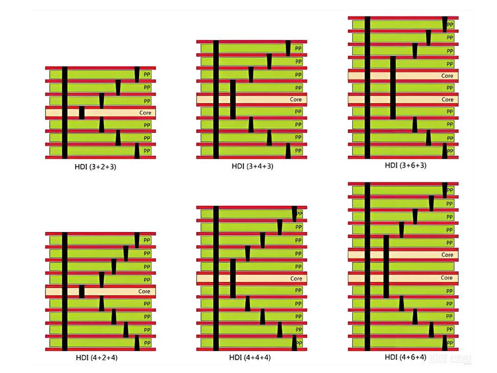
3. HDI PCB Stackup: Step-by-Step Layer Planning
3.1 Choosing HDI Order Structures (1+N+1 vs. 2+N+2)
- 1+N+1: 1 microvia layer per side + N core layers (ideal for 6-8 layer PCBs, cost-effective for consumer devices)
- 2+N+2: 2 microvia layers per side + N core layers (supports 10-20+ layers for industrial/medical gear)
Example: A smartphone uses a 2+4+2 HDI PCB stackup (2 outer microvia layers + 4 core layers) for density and cost balance.
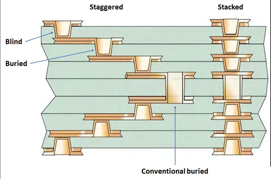
3.2 Blind/Buried Via Stacking Strategies
- Stacked vias: Aligned vertically (saves space, requires precision lamination—best for high-reliability medical devices)
- Staggered vias: Offset (more forgiving for manufacturing, uses slightly more space)
Resin-plug stacked vias to prevent moisture ingress in harsh environments.
3.3 Material Selection for HDI PCB Design
- High-frequency apps: Low-loss dielectrics (Rogers 4350B, Isola S1000-2M) to minimize signal attenuation
- Harsh environments: Tg170°C+ substrates (resist warping in automotive/industrial use)
- Eco-friendly designs: RoHS-compliant materials (cellulose substrates, ENIG lead-free plating)
3.4 Impedance Control for High-Speed Designs
Aim for 50Ω (signal traces) or 100Ω (differential pairs) in HDI PCB design. Use tools like Altium Designer’s impedance calculator to adjust trace width, dielectric thickness, and copper weight—then validate with your HDI PCB manufacturing partner to account for process variations.
4. Microvia Design Best Practices to Avoid Failures
4.1 Stick to Aspect Ratio Limits
Microvia design in HDI PCB design requires an aspect ratio ≤1:1 (depth ≤ diameter). For example, a 0.075mm diameter microvia should not exceed 0.075mm depth—exceeding this causes poor plating and open circuits.
4.2 Pad Size Rules for Laser-Drilled Holes
Add 6mil (0.15mm) to the microvia diameter for pad size. A 3mil (0.075mm) microvia needs a 9mil (0.225mm) pad to prevent delamination and ensure strong copper bonding.
4.3 Clearance Requirements
- Outer layers: 6mil clearance between microvias and traces; 10mil from board edges
- Inner layers: 4mil clearance (confirm with your HDI PCB manufacturing partner’s DFM guidelines)
4.4 Plating vs. Resin Plugging
- Plated microvias: For signal paths (conductive, cost-effective)
- Resin-plugged microvias: For via-in-pad designs (flat surface for soldering, prevents solder wicking)
5. HDI DFM: Manufacturability Checklist
5.1 Line Width/Spacing Tolerances
Stick to 3mil/3mil (0.075mm/0.075mm) for mass production. 2mil/2mil is possible but increases costs and reduces yield—only use for specialized high-density apps.
5.2 Prevent Over-Etching
Use rounded trace corners (avoid sharp angles) and add a 1mil buffer to trace widths. This compensates for etching variations and prevents narrow, high-resistance traces.
5.3 Ensure Lamination Alignment
Specify ≤50μm (0.05mm) layer shift tolerance. Use alignment pins and symmetrical HDI PCB stackup to reduce stress during lamination—critical for multi-layer HDI PCB design.
5.4 X-Ray Testability for Hidden BGAs
Add X-ray test points near BGA pads (uncovered by solder mask) to verify solder joints. Hidden BGAs in HDI designs can’t be inspected visually—test points catch defects early.
6. BGA Fanout HDI: Expert Techniques
6.1 Via-in-Pad for Fine-Pitch BGA (0.4mm Spacing)
Place microvias directly under BGA pads, then resin-plug them for a flat soldering surface. Match pad size to BGA ball diameter (e.g., 0.2mm pad for 0.4mm spacing BGAs).
6.2 ELIC Routing for Cost Savings
Enhanced Low-Cost Interconnect (ELIC) uses blind vias to route BGA signals to inner layers, eliminating expensive stacked microvias. Ideal for mid-range consumer devices.
6.3 Skip Vias to Save Space
Skip vias bypass 1+ inner layers (e.g., top layer to 3rd layer), freeing up inner layer space for other traces. Perfect for high-layer-count HDI PCB design.
6.4 Reduce Parasitic Capacitance/Inductance
Keep high-frequency trace lengths <10mm, use differential pairs, and avoid stubs. Add adjacent ground planes to absorb interference and improve signal integrity.
7. Thermal Management in High-Density HDI Layouts
7.1 Copper Balancing
Balance copper weights across layers (e.g., 1oz copper on top/bottom layers, 0.5oz on inner layers) to prevent warping and distribute heat evenly.
7.2 Thermal Relief Pads for Power Components
Use thermal relief pads (narrow copper spokes connecting to ground planes) for voltage regulators and LEDs. For high-power parts, use solid pads with thermal vias.
7.3 Thermal Vias & Embedded Heat Sinks
Place thermal vias in a 1mm-spaced grid under power components (10-20 vias per part). Embedded copper heat sinks reduce temperatures by 20-30°C for industrial/automotive apps.
7.4 Thermal Simulation Tools
Use ANSYS Icepak or Cadence Celsius to predict hotspots before finalizing HDI PCB design. Adjust component placement or add thermal features early to avoid redesigns.
8. Top HDI PCB Design Software for 2026
8.1 AI-Driven Auto-Routing Tools
- Altium Designer ($7k+/year): Best for professional engineers—AI auto-routing handles BGA fanout HDI and signal integrity optimization.
- Zuken CR-8000 ($10k+/year): Ideal for 10+ layer HDI designs with advanced simulation.
8.2 DFM Verification Plugins
- Mentor Graphics Valor NPI: Scans designs against HDI PCB manufacturing rules in real time.
- Altium DFM Checker: Flags line width/clearance issues before production.
8.3 3D Modeling Tools
- SolidWorks PCB: Visualizes HDI PCB stackup to identify layer alignment and component clearance issues.
- Altium 3D Viewer: Collaborates with mechanical teams for enclosure fit.
8.4 Cost-Effective Alternatives
- KiCad (free): Suitable for small businesses/hobbyists with basic HDI needs.
- Eagle ($699+/year): Balances features and cost for mid-range designs.
9. Common HDI PCB Design Mistakes & Fixes
9.1 Underestimating Manufacturing Capabilities
Mistake: Specifying 2mil/2mil traces when your factory only supports 3mil/3mil.
Fix: Share designs early with HDI PCB manufacturing partners and follow their HDI DFM guidelines.
9.2 Ignoring CAF Risk
Mistake: Tight via spacing (≤0.3mm) causes Conductive Anodic Filament (CAF) growth.
Fix: Use high-Tg substrates, maintain ≥0.5mm via spacing, and avoid vias near board edges.
9.3 Misaligned Blind/Buried Vias
Mistake: Poor lamination leads to via misalignment and signal loss.
Fix: Add fiducial marks, specify ±25μm layer shift tolerance, or use staggered vias.
9.4 Non-Compliant Materials
Mistake: Using tin-lead plating (non-RoHS) or low-Tg substrates for harsh environments.
Fix: Choose ENIG lead-free plating and Tg170°C+ substrates for global compliance.
10. HDI PCB Design Case Studies
10.1 Smartphone Motherboard (12-Layer HDI)
Challenge: Fit 5G modem + BGA in a 60x80mm footprint.
Solution: 2+8+2 HDI PCB stackup, via-in-pad for 0.4mm BGA, and ELIC routing.
Result: 40% smaller board, 98% yield rate, and 10% better signal integrity.
10.2 Automotive Radar (8-Layer HDI)
Challenge: Withstand -40°C to 125°C temperatures and high vibration.
Solution: Tg180°C substrate, thermal vias for power components, and resin-plugged stacked vias.
Result: Zero failures in 10k+ hours of testing, RoHS compliance.
10.3 Wearable Device (6-Layer HDI)
Solution: 1+4+1 stackup, microvias (0.075mm), and copper balancing.
Result: 35% lighter board, 96% yield, and 20% longer battery life.
11. FAQ: Top 7 HDI PCB Design Questions Answered
Q1: What’s the minimum microvia diameter for mass production?
Q2: How to fix layer shift in 3rd order HDI designs?
Q3: Can HDI PCBs support 20+ layers reliably?
Q4: What’s the cost difference between 1st and 2nd order HDI?
Q5: How to improve signal integrity in high-speed HDI designs?
Q6: What DFM rules are non-negotiable for HDI?
Q7: Are there eco-friendly HDI materials?
12. 2026 HDI PCB Design Trends to Future-Proof Your Projects
12.1 AI-Driven Design Automation
12.2 SiP Integration
12.3 16+ Layer HDI for AI Servers
12.4 Green Manufacturing
Ready to Bring Your HDI PCB Design to Life?
You’ve got the expertise—now partner with a manufacturer that delivers precision, reliability, and on-time results. Our team specializes in HDI PCB design manufacturing for 5G, automotive, wearable, and industrial applications, with 98% yield rates and RoHS/WEEE compliance. We handle 6-20+ layer HDI designs, from prototype to mass production, and offer free DFM reviews to fix issues before manufacturing. Don’t let subpar manufacturing ruin your hard work—send your design files to sales@pcbtry.com today, and we’ll deliver high-performance HDI PCBs that meet your specs, budget, and timeline. Let’s turn your vision into reality.


0 Comments