
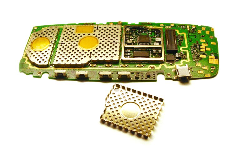
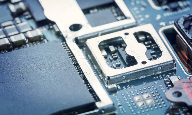
PCB Shielding Cans, also known as board-level EMI shielding enclosures, isolate sensitive circuits by forming a localized Faraday cage on the circuit board, reducing electromagnetic interference. In practical design, they are broadly divided into integrated shielding cans and split (frame + cover) shielding cans. The most common integrated shielding cans are directly soldered to the PCB ground pads, providing stable and efficient shielding performance, making them the preferred solution for most consumer electronics and industrial products.
Typical board-level shielding cans consist of a stamped metal enclosure connected to the PCB’s ground plane through ground pads or vias. Some applications use continuous welding to form a completely enclosed structure, achieving the highest level of electromagnetic shielding. More flexible methods are also available, such as placing solder pads every 2–4 mm along the shielding edge or using through-hole pins, depending on the EMI requirements of different devices.
Integrated board-level shielding cans offer the advantages of low cost, simple structure, and strong shielding effect. Whether for prototyping or mass production, we can provide customers with high-precision, multi-specification EMI/RFI shielding can manufacturing services.
What exactly is a PCB shielding cover?
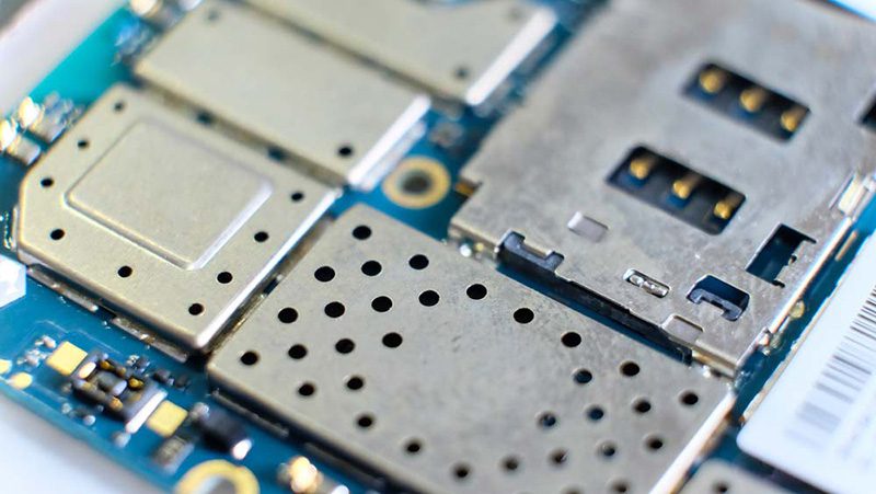
PCB shielding covers, typically made of aluminum, nickel-silver alloys, or copper alloys, are used to cover and protect components in specific areas of a PCB from external electromagnetic interference (EMI). They form a Faraday cage through grounding, helping electronic equipment pass EMC testing (immunity and radiation testing).
Typical characteristics of shielding covers in PCB design include:
Low profile: Suitable for areas with limited height.
Thin metal molding: Lightweight and low cost, but limited mechanical reinforcement.
Non-contact design: Sufficient internal clearance is required to avoid contact with components.
Multiple mounting options: SMD mounting is most common, but through-hole versions are also available.
High assembly requirements: Some shielding covers require manual soldering, and in some cases, low-temperature soldering is necessary.
Customers can choose standardized shielding covers or fully customized models to suit different form factors, layouts, and EMI requirements.
How to properly ground the PCB shielding layer?
Effective EMI shielding relies on proper grounding design. Depending on the product architecture, grounding methods are generally categorized into three types:
- 1. Single System Ground:
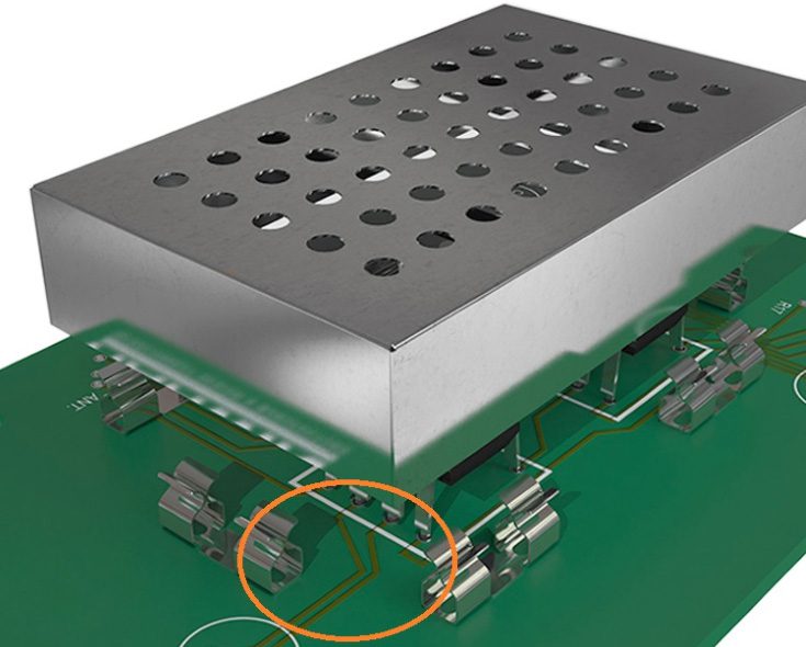
The shielding layer is directly connected to the system ground plane. A common practice is to place grounding vias near the shielding pads to ensure a continuous current return path; this is the method used in the vast majority of electronic products.
- 2. System Ground + Chassis Ground:
If the shielding layer is required to also provide ESD protection, it can be connected to the chassis ground. However, the shielding layer is usually located within the board, while the chassis ground is at the board edge, requiring extra attention to common-mode noise generation. A common practice is to add a chassis ground ring around the sensitive area.
- 3. Isolated System:
In isolated power supplies or precision analog systems, the shielding layer can only be connected to one grounding network; it must never be connected across two grounds simultaneously, otherwise electrical isolation will be compromised and severe interference will occur.
Key considerations for PCB shielding design
When designing PCB shielding structures, multiple factors must be considered comprehensively to ensure that electromagnetic interference (EMI) is suppressed without affecting circuit functionality, heat dissipation, or manufacturability.
- 1. EMI Frequency Range
First, the interference frequencies that need to be suppressed must be clearly defined. Different shielding materials and structures have significantly different effectiveness at high and low frequencies; therefore, the shielding strategy must be formulated based on the target frequency band.
- 2. Shielding Location and Coverage Area
Identify the areas on the PCB that are most susceptible to or likely to generate EMI, and ensure that the shielding cover accurately covers these areas. The shielding structure should be as close as possible to the interference source or sensitive components to achieve optimal suppression.
- 3. Material Selection
The conductivity, magnetic permeability, thickness, and cost of the shielding material directly affect shielding performance and production costs. Common materials include aluminum, copper, nickel-iron alloys, steel, and conductive coatings. The optimal solution should be selected by comparing the interference frequency band, weight, and budget.
- 4. Shielding Integrity and Structural Completeness
Effective shielding must maintain a continuous, enclosed structure, minimizing gaps, openings, and discontinuities. Seams, solder joints, and mechanical openings should be kept to a minimum to ensure that no EMI leakage paths are created.
- 5. Heat Dissipation and Thermal Management
Shielding covers may hinder component heat dissipation, especially when the material has low thermal conductivity or the internal space is small. Therefore, heat dissipation paths must be considered in the design, including ventilation holes, heat-dissipating copper traces, or structural thermal management solutions, to prevent heat accumulation caused by shielding.
- 6. Manufacturability and Assembly Method
The shielding structure must be easy to mass-produce and assemble, including:
Whether it is suitable for standard SMT processes
Whether reflow soldering affects the rework of internal components
Whether it will incur additional material or labor costs
A reasonable design should ensure a balance between EMI shielding and production efficiency.
Other poor grounding methods
In practical projects, the grounding method of the shielding structure is often overlooked. However, improper grounding design can easily lead to increased noise, excessive radiation, and even turn the shielding layer itself into a new source of interference. Common incorrect grounding methods include:
Using a capacitor to connect the shielding layer to ground:
This method reduces high-frequency radiation to some extent, but it may also introduce low-frequency coupling problems, creating risks across a wider bandwidth.
Connecting an RC network in series between the shielding layer and ground:
This design usually reduces the impedance of high-frequency signal paths, but it may create new resonant paths, thus promoting an increase in low-frequency radiated emissions.
The shielding layer is completely floating:
If the shielding layer is not grounded, it will act like a large antenna, re-radiating any coupled energy, making EMI even worse.
The best practice is simple: use a low-impedance, direct grounding method, making the shielding layer a three-dimensional extension of the PCB ground plane. Maintaining a low impedance between the shielding layer and ground not only significantly improves the shielding effect but also avoids introducing additional noise paths.
The difference between PCB shielding cans and EMI shielding cans
Although PCB shielding cans and EMI shielding cans are often used interchangeably, their applications are not entirely the same:
| Types | Main functions: | Applications |
| PCB Shielding Cans | Isolate and protect local circuits within the PCB | High-frequency devices, sensitive analog circuits, small area isolation |
| EMI Shielding Cans | Provide comprehensive EMI immunity for the entire device or system | End product housings, power systems, wide-area electromagnetic protection |
PCB shielding containers are used for localized shielding, while EMI shielding containers are used for system-level shielding. The choice depends on the electromagnetic characteristics of the device and the target application.
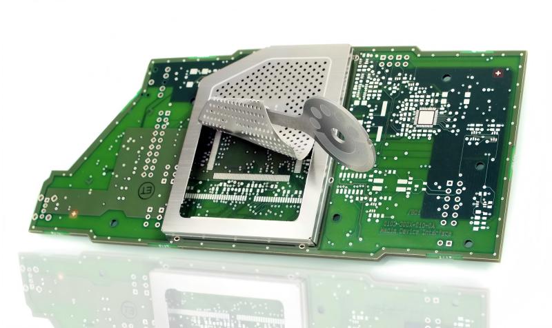
Disadvantages of integrated PCB shielding
While integrated shielding offers advantages such as high efficiency and low cost, it also presents some significant limitations in production and maintenance:
- Difficulty in inspection and rework after reflow soldering:
The shielding covers the components, obstructing visual inspection and probe contact. Post-soldering troubleshooting becomes difficult.
- High cost and risks in post-soldering installation:
Manual soldering increases costs and may cause adjacent components to detach or suffer heat damage. Disassembly and replacement are also difficult.
- Strict coplanarity requirements:
The solder joints between the shielding and the PCB need to be highly flat to ensure reliable contact. As the size of the shielding increases, the manufacturing difficulty increases significantly.
Chemical etching PCB shielding
Our chemical etching process boasts industry-leading advantages, significantly enhancing the functionality of RF/EMS shields while reducing overall manufacturing costs. Compared to traditional stamping processes, chemical etching eliminates the need for molds or die preparation, drastically shortening lead times and making it ideal for applications ranging from rapid prototyping to mass production.
This process also offers high design flexibility, easily integrating ventilation holes, access holes, bending guide lines, part numbers, and markings, with virtually no additional cost.
Material selection and processing capabilities
In terms of RF shielding materials, nickel-silver alloy is the most commonly used choice due to its excellent cost-effectiveness. It offers good weldability and strong oxidation resistance, usually eliminating the need for further electroplating. In addition to nickel-silver alloy, we also offer a variety of other metal materials such as brass and low-carbon steel, and maintain a stable inventory.
To provide a complete solution, we possess comprehensive in-house processing capabilities including forming, assembly, spot welding, and electroplating. Our electroplating options cover various processes such as tin, silver, nickel, and gold, meeting different application scenarios and performance requirements, ensuring the delivery of high-quality RF shielding products to our customers.
PCB shielding has become a core method in modern electronic devices for ensuring EMC compliance, suppressing crosstalk, and protecting sensitive signal chains. From grounding strategies and type selection to manufacturing and assembly, every aspect directly impacts the final shielding effect. By rationally planning PCB stack-up, layout and routing, copper design, and grounding schemes, engineers can significantly reduce system EMI risks, minimize rework costs, and improve product reliability.
As a supplier deeply rooted in PCB design and manufacturing, Thindry provides customers with full-process technical support from initial solution planning to mass production, including shielding design, EMC optimization, thermal layout, and stack-up recommendations. This helps customers avoid potential risks in the early stages of product development and achieve high-quality, compliant electronic products.


0 Comments