
Main PCB assembly is the core embodiment of the performance, stability, and reliability of electronic products. It integrates circuit design achievements, technological advancements, and precision manufacturing capabilities. The following article provides a comprehensive analysis of motherboard PCB assembly, delving into key components, the complete manufacturing process, cost influencing factors, and the innovative technologies and challenges reshaping the industry’s future, presenting you with a professional and practical motherboard assembly technical guide.
What does main PCB board mean?
The main PCB refers to the most core and critical printed circuit board in an electronic device, serving as the functional center and communication hub of the entire system. It carries key components such as the CPU, memory, power management, and electrical interfaces, providing the computing, control, and signal transmission capabilities required for the device to operate. Whether it’s consumer electronics or industrial equipment, the main PCB is the fundamental platform for product design and function implementation, and a core component in any electronic system.
Understanding the importance of the main PCB
The main PCB assembly is the core hub of electronic devices, playing a crucial role in function control, data flow, and system coordination. Its importance lies not only in the structure of the circuit board itself but also in its function as a platform for internal communication, signal processing, and function integration within the device. The main board assembly process is far more than just soldering components or connecting wires; it is an engineering practice that integrates performance, stability, and reliability, directly determining the quality and user experience of the final product.
What are the characteristics of the main PCB assembly?
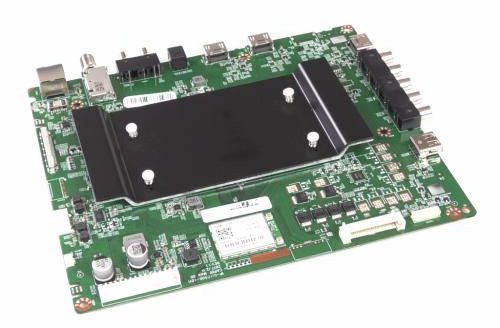
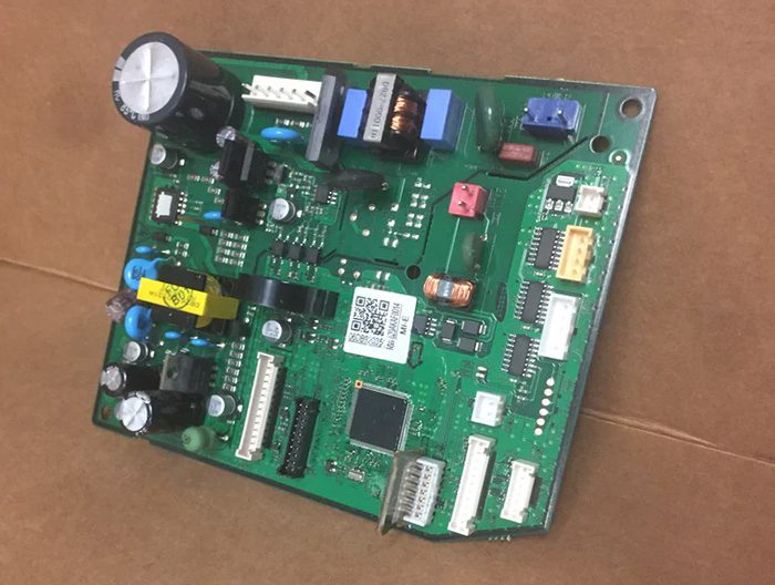
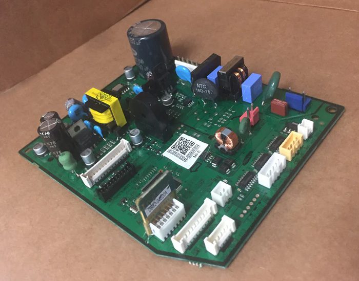
The Main PCB Assembly refers to the main control circuit board in a complete system that performs core control tasks and has already completed component assembly and debugging. It is not just a bare PCB, but a fully functional core control module that can be directly put into use.
- 1. System Core Control Center
The Main PCB Assembly integrates the main processor, control chips, memory, and communication interfaces, acting as the “central brain” of the device, responsible for processing key logic, data, and signal coordination.
- 2. Complete Circuit Assembly
Unlike PCBs without assembled components, the Main PCB Assembly has completed SMT, DIP component insertion, and necessary debugging and testing, allowing for seamless integration into the complete system.
- 3. High-Density, High-Integration Design
The main control board typically uses a multi-layer PCB structure with dense wiring and concentrated functional modules, requiring higher precision in manufacturing, soldering processes, and quality control.
- 4. System Connection Hub
As the central node of the system, the Main PCB Assembly provides electrical connections to multiple sub-boards and peripherals, including:
FPC/FFC interfaces
Board-to-board connectors
External ports such as USB and Ethernet
Responsible for communication, power supply, and signal interaction between various modules.
- 5. Subject to Rigorous Quality and Reliability Testing
The main control board undergoes FCT functional testing, aging testing, and reliability verification such as EMC/ESD testing according to product requirements to ensure long-term stable operation.
- 6. Highly Customized, Tied to Specific Product Models
The layout, size, and functionality of the Main PCB Assembly are usually deeply integrated with the complete system and are customized designs, making them unsuitable for direct use in other product models.
Analysis of the Main PCB Board Structure: Core Components and Structure
To thoroughly understand the working principles of the main PCB, it is necessary to first grasp its basic structure and core components. The main substrate of the PCB is FR4, made of glass fiber reinforced epoxy resin, which has excellent mechanical strength and insulation properties. When thin copper foil is laminated onto the surface of the substrate and etched into conductive traces, it forms the basic circuit structure that carries electronic signals.
A complete main PCB assembly (PCBA) typically consists of the following parts:
1. Substrate (FR4)
Serving as the structural support and insulation core of the circuit board, providing a base layer for all copper traces and components.
2. Copper Foil Layers
Copper clad and etched to form electrical circuits, used for signal transmission and power distribution.
3. Solder Mask Layer
A protective coating covering the surface of the traces, preventing short circuits, solder bridging, and oxidation. Common colors include green, blue, black, and purple.
4. Silkscreen Layer
Used to mark component locations, models, test points, and other information for easy assembly and maintenance.
5. Active Components
Including ICs, MCUs, DSPs, memory chips, etc., which are the core execution units of the circuit’s functions.
6. Passive Components
Such as resistors, capacitors, inductors, and crystal oscillators, used for basic circuit functions such as filtering, voltage regulation, timing, and tuning.
7. Connectors and Interfaces
Including power connectors, USB, HDMI, network ports, FPC/FFC, board-to-board connectors, etc., enabling internal and external signal/power connections for the entire device.
8. Electromechanical Components
Such as switches, relays, and fans, used to perform physical actions or provide cooling and control capabilities.
The main differences between a motherboard and a main PCB board.
A PCB (Printed Circuit Board) is a general concept referring to any circuit board that mounts electronic components and carries electrical circuits. A “motherboard,” however, is a specific type of PCB, typically used in computer systems, serving as the core control and connection platform for the entire system. “Main PCB” is not a standard term, and is more often used to refer to the main functional circuit board in non-computer devices such as televisions, cameras, and printers.
The main differences between a motherboard and a main PCB are as follows:
- Different application scope
A motherboard specifically refers to the core PCB in a computer; while a main PCB can refer to the main control board in any electronic device, and is closely related to a specific industry or product.
- Significant difference in complexity
Motherboards typically have more layers, denser wiring, and include various expandable interfaces (such as PCIe, memory slots, M.2, etc.) to support upgrades and expansion.
Main PCBs are usually customized for specific functions, with higher integration and a more compact structure, but weaker expansion capabilities.
- Different component types
Motherboards typically include complex components such as a CPU socket or soldered CPU, chipset, memory slots, and BIOS/UEFI firmware.
In main PCBs, the processor and control ICs are usually directly soldered onto the board, and may not require a separate “chipset” structure; their design is more specialized.
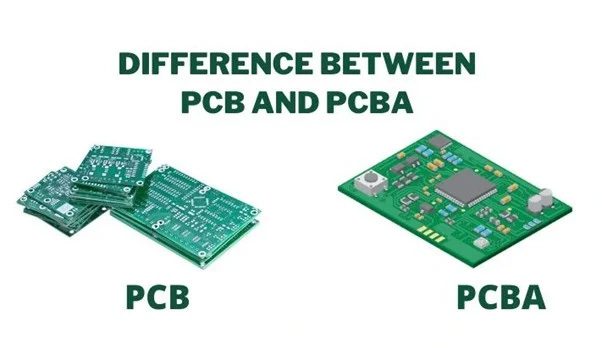
What is the difference between a PCB and a main PCB assembly?
| Comparison Dimensions | PCB | Main PCBA Assembly |
| Stage | Basic bare board, only PCB manufacturing completed | Finished circuit board with components mounted and soldered |
| Functionality | No functionality, only possesses circuit structure | Possesses full electrical functionality and can be directly used in equipment |
| Components | No components | Includes all components such as ICs, resistors, capacitors, and connectors |
| Appearance | Flat board material with copper foil and solder mask layer | Three-dimensional structure with a large number of electronic components |
| Manufacturing Process | PCB manufacturing processes including lamination, etching, drilling, plating, solder masking, and silkscreen printing | PCB manufacturing + SMT assembly + DIP insertion + reflow soldering/wave soldering and other assembly processes |
| Testing Methods | Flying probe testing, impedance testing, AOI circuit inspection | AOI surface mount inspection, X-Ray (such as BGA), ICT in-circuit testing, functional testing, and burn-in testing. |
| Cost Drivers | Number of layers, materials (FR4/Rogers, etc.), via density, surface treatment | Includes PCB cost + component cost + SMT/DIP assembly cost + advanced testing cost |
| Relative Cost | Relatively low cost | Approximately 5–10 times higher than the PCB (depending on complexity) |
How is the main PCB assembly manufactured?
The production of Main PCB Assemblies is a high-precision, high-reliability process that requires advanced equipment and strict quality control. The overall process typically includes the following steps:
- Solder Paste Printing
Solder paste is precisely applied to the solder pads using a stainless steel stencil, providing positioning and a welding base for component placement.
- SMT Placement
Using high-speed placement machines and vision alignment systems, components such as resistors, capacitors, and ICs are accurately placed onto the solder paste areas. Modern equipment can achieve placement speeds of tens of thousands of components per hour.
- Reflow Soldering
The circuit board enters the reflow soldering oven, going through stages such as preheating, constant temperature, reflow, and cooling, allowing the solder paste to melt and form reliable solder joints.
- Through-Hole Component Insertion (DIP)
Larger components or those requiring mechanical stress resistance, such as connectors, transformers, and relays, are inserted through pre-drilled holes. This can be done manually or by automated equipment.
- Inspection and Testing
AOI: Detects component placement deviations, missing components, and solder joint defects.
X-Ray: Inspects invisible solder joints such as those on BGAs.
ICT / FCT: Verifies electrical performance and functionality against design specifications.
These are crucial steps in ensuring reliability.
- Final Processing and Protection
After assembly and testing, protective coatings, such as conformal coating, can be added as needed to enhance moisture resistance, dust protection, and environmental durability. This is especially critical for high-end applications such as aerospace and medical instruments.
One-stop integrated service for PCB motherboard assembly
Thindry is a leading one-stop service provider for PCB motherboard assembly in China, covering the entire process from PCB design and manufacturing to component procurement and finished product assembly. Through an intelligent production system and efficient supply chain management, Thindry effectively reduces costs and shortens delivery times, making it the ideal choice for those seeking a high-quality PCB motherboard assembly manufacturer.
- Industry Expertise and Experience
With over 20 years of experience in PCB and SMT manufacturing, Thindry can confidently handle various needs, from prototype production to mass production. A professional team of engineers provides comprehensive technical support throughout the process, ensuring product quality and design reliability.
- Advanced Equipment and Intelligent Manufacturing
Thindry utilizes advanced systems such as CRM/MES/ERP/IoT for intelligent factory management and is equipped with comprehensive SMT defect detection, ESD electrostatic protection, and full-process quality tracking systems, ensuring that every motherboard is of exceptional quality.
- Certified Quality Assurance
The company is certified with international quality systems such as ISO9001, IATF16949, and ISO13485, and strictly adheres to industry standards in production, making it a trustworthy professional PCB assembly partner.
- Attentive and Efficient Customer Service
Thindry provides fast-responding 24/7 customer support, ensuring that you receive timely and professional answers regarding PCB motherboard assembly quotations, technical consultations, and order progress.


0 Comments