
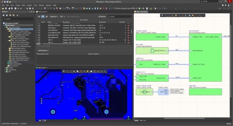
Customers ordering printed circuit boards (PCB) need to provide precise and detailed information about the board design and specifications. Therefore, standardized and compliant PCB file formats are crucial. Only with complete design documentation can the production process proceed smoothly. Key documents including circuit schematics, bill of materials (BOM), PCB layout diagrams, and layer stack-up information are essential for ensuring that the design intent is correctly understood and ultimately successfully implemented.
Why is a specific file format required when ordering PCB?
In PCB manufacturing, file formats not only affect information transmission but also manufacturing accuracy and efficiency. Therefore, understanding and mastering standard file formats such as Gerber is crucial, primarily in the following three aspects:
- 1. Standardized Transmission:
A unified PCB file format ensures that design data is transmitted to manufacturers in a standardized, clear, and industry-standard manner, avoiding misunderstandings and improving communication efficiency.
- 2. Providing Complete Details:
These files contain all the core information needed for PCB manufacturing, including component locations, electrical connections, routing methods, layer stack-up, and drill locations. Detailed data is a prerequisite for accurate production.
- 3. Ensuring Software Compatibility:
Different PCB design software generates different files, and manufacturers typically need compatibility with multiple tools. Using standard formats reduces conversion errors and lowers production risks.
What documents are needed for PCB manufacturing?
- 1. Fabrication Drawing
The fabrication drawing contains the PCB’s mechanical dimensions, layer stack-up, tolerance requirements, and key annotations, serving as a crucial basis for the production process. It ensures that the manufacturer can process the PCB according to the design intent, ensuring the final product meets structural and performance specifications.
- 2. Bill of Materials (BOM)
The Bill of Materials lists all required components, including model number, quantity, package, and supplier part number. The BOM helps manufacturers accurately procure components and ensures the use of correct and consistent materials during assembly.
- 3. Pick-and-Place File
The pick-and-place file records the precise coordinates, rotation angle, and name of each component on the PCB. Automated placement equipment uses this data to complete the rapid and accurate assembly of components, thereby reducing assembly deviations and improving production efficiency.
PCB schematic file format types
| File Types: | Description |
| Gerber Files | Gerber files are primarily used for PCB layout and manufacturing processes. |
| Schematic Capture Files | They are typically saved with the “.SCH” extension. These files contain all the details of the schematic, including components, component connections, and other relevant design information. |
| SPICE Netlist Files | They list the electrical connections between all components, demonstrating how the circuit will operate in a practical application. |
| PDF or Image Formats | For ease of documentation or review, schematics are usually exported as PDF or image files (such as PNG or JPEG). |
The main differences between netlists and schematics
| Aspects | Schematic Design File (.dsn) | Netlist file |
| Format | A binary or proprietary file format used for software. | Plain text, standardized format |
| Scope | A complete schematic design, including symbols and metadata. | This refers only to connections between components |
| Usage | Editable within circuit schematic design tools for circuit construction. | PCB layout tools read data to guide component placement and routing |
| Components and Networks | Includes components, their properties, and connections. | Focus only on the connections between component pins |
| Readability | Primarily presented visually, but editable within the design tool. | Text-based, easy to parse, but lacks visual editing capabilities |
Why file formats are important in PCB manufacturing
Providing accurate, complete, and standardized documentation is crucial for manufacturers during PCB manufacturing and assembly. Any missing, improperly formatted, or incorrectly formatted documents can lead to production delays, assembly discrepancies, additional costs, and even batch scrapping. The following are the key documents and their roles in the manufacturing process:
Copper Layer Documents: Define trace routing and electrical signal transmission paths, forming the core foundation of circuit functionality.
Placement Documents: Provide component coordinates and angle information, ensuring accurate, fast, and reliable component placement by SMT equipment.
Manufacturing Drawings: Contain information such as board thickness, hole diameter, tolerances, solder mask, and mechanical dimensions, ensuring that the finished product dimensions match design requirements.
What are the differences between PCB design and schematic design?
While PCB design and schematic design are closely related, their roles, content, and application scenarios are quite different.
- 1. Different Purposes and Contents:
Schematic design focuses on the logical structure and electrical behavior of a circuit. Through symbols such as power supplies, components, and signal lines, it illustrates how the circuit works internally, facilitating engineers’ functional analysis, verification of logical relationships, and troubleshooting.
PCB design, on the other hand, translates the electrical connections in the schematic into the physical layout of the actual circuit board. It focuses on the actual size, location, routing, and layer stack-up of components, providing an executable blueprint for PCB manufacturing and assembly.
- 2. Different Application Scenarios:
Schematic design is commonly used in R&D, debugging, and later maintenance, serving as a crucial document for understanding product operating principles and troubleshooting.
PCB design documents, however, are the foundational data for actual PCB production, SMT assembly, and electrical testing, directly impacting manufacturing quality and product performance.
In summary, the schematic is the starting point for electronic product development, defining the logical relationships of the circuit; while PCB design is responsible for realizing this logic into a manufacturable physical circuit board, serving as the crucial bridge between “circuit concept” and “physical product.”
How to process your PCB design files
At Thindry, we understand that accurate and standardized design documents are the core foundation for smooth and efficient PCB manufacturing. To this end, our engineering team maintains close communication with clients to ensure that all submitted materials (including schematics, Gerber files, etc.) are correctly formatted and complete, allowing for seamless integration into the manufacturing process.
When you entrust your PCB project to Thindry, we offer:
- Comprehensive File Format Support:
Regardless of whether you use Altium, Eagle, KiCAD, or other mainstream design software, we can read and process your schematics and PCB design files.
- Pre-Production Engineering Review (DFM Review):
Before production begins, our engineers rigorously review schematics, Gerber files, drilling information, and other relevant documents to identify potential problems early and avoid rework and delays.
Flexible Document Submission Methods:
In addition to standard design files, we also accept PDF documents for quick reference during production communication.
Choosing the correct PCB file type is a crucial step in ensuring a smooth manufacturing process. From .SCH schematic files to Gerber and SPICE netlists, each format plays a crucial role between design and production. Thindry supports multiple file formats, helping you easily submit designs and ensuring high-quality PCB deliverables.
If you need assistance with PCB design or are ready to put your project into production, please feel free to contact Thindry. We will provide you with reliable and efficient manufacturing services.
What challenges are there in PCB file and data exchange?
In the data exchange process between PCB design and manufacturing, file format, naming conventions, and data completeness often become key factors affecting schedule and quality. Failure to identify and address these issues in advance can easily lead to rework, delays, and even manufacturing errors during the production stage. The following are common challenges and their causes:
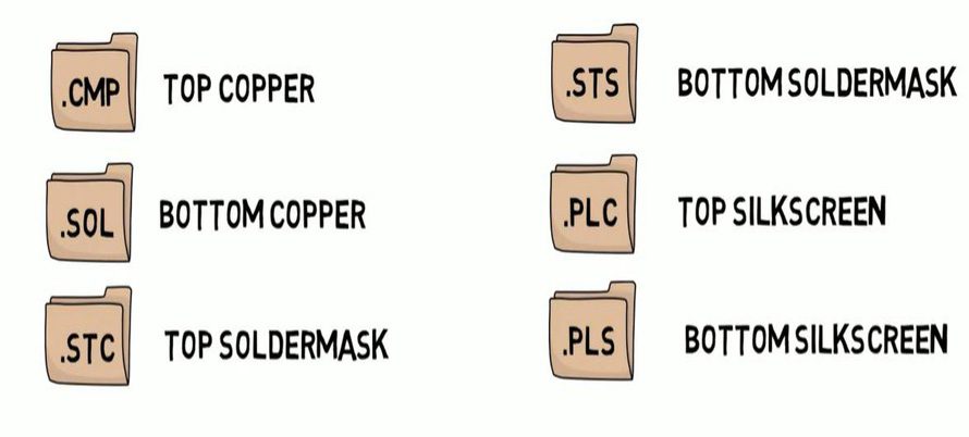
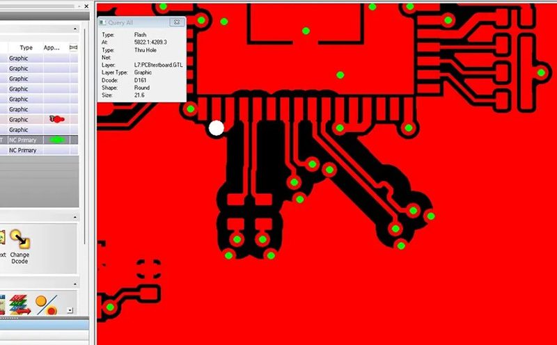
- 1. Incomplete Gerber Layer Files
Before submitting to the manufacturer, it is essential to ensure that each layer of the Gerber file is complete and accurate. For example, if a silkscreen layer is missing, the manufacturer will often assume that the layer does not need to be manufactured, resulting in a discrepancy between the finished product and the design. File type and naming conventions directly affect the manufacturer’s interpretation of layer files, therefore, they must be rigorously checked.
- 2. Inaccurate Component Placement Information
If the pick-and-place/centroid file is not synchronized with the latest design, coordinate errors, mismatched rotation angles, and other issues may occur. Once the design is modified, both the Gerber file and the centroid file must be updated synchronously; otherwise, it will cause component misalignment or assembly errors.
- 3. Vague or Non-standard Naming Rules
Unclear file naming significantly increases communication costs, making it difficult for the manufacturer to understand the file content and its correspondences. This not only affects data parsing but can also lead to production delays. Standardized naming conventions can significantly improve the efficiency and accuracy of the entire delivery chain.
- 4. Incomplete or Incorrect Documentation
Even if documents are successfully transmitted, problems may arise due to outdated material information, missing component numbers, or inconsistent document versions. Unreviewed BOM, drawings, or specifications can create risks during production and assembly. Therefore, a thorough check before formal submission is crucial.
FAQ
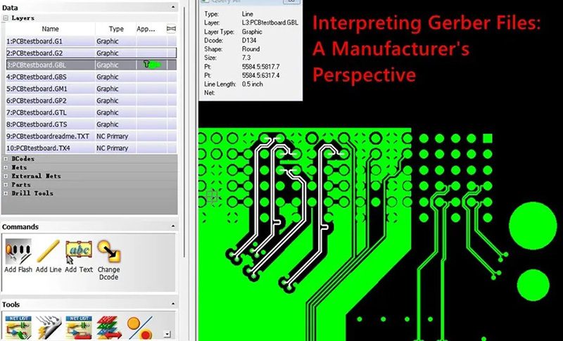
Q1. Which software can open Gerber files?
Common Gerber viewing tools include Gerbv, ViewMate, KiCad Gerber Viewer, etc., which can be used to check whether the layer information is complete and whether the layout is correct.
Q2. How to export a PCB design as Gerber format?
In EDA software such as Altium Designer, KiCad, and Cadence Allegro, Gerber can be generated through the “File → Fabrication Output” or “Manufacture → Export” options. Before exporting, please ensure that the layer selection, drilling data, and unit settings are accurate.
Q3. What documents are required to submit to the PCB manufacturer?
Generally, the manufacturer needs:
Gerber files (each layer)
Excellon drill files (.drl)
Pick-and-Place files
These documents are sufficient for the manufacturing needs of most prototype boards and standard PCB.
Q4. How to verify the accuracy of exported files before production?
It is recommended to use the CAM viewer built into the EDA software or a third-party Gerber verification tool for checking. Pay special attention to:
Layer alignment: Is it correct?
Missing drill holes?
Mirrored text?
Abnormal polarity and pad shape?
Q5. How to better organize PCB output files?
Best practice is to create a compressed folder named after the project, containing:
Gerber files for each layer
Drill files (.drl)
Manufacturing instructions or README (layer stack-up, units, board thickness, etc.)
Surface mount files & BOM (if assembly is involved)
A clear organizational structure can prevent communication breakdowns during quoting and manufacturing.


0 Comments