
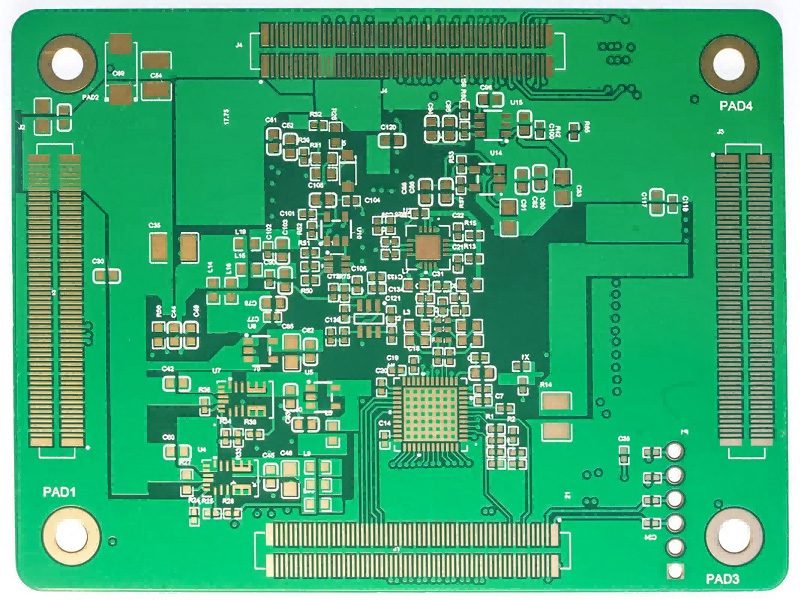
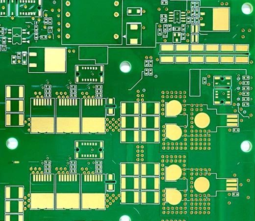
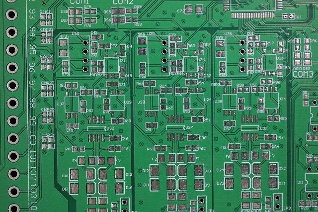
In PCB design, exposed copper refers to the area of copper foil directly exposed, not covered by solder mask.
Typically, PCB surfaces are coated with a solder mask to protect the copper foil from oxidation, prevent short circuits, and improve overall reliability. However, in certain functional areas, the copper foil must remain exposed to perform electrical or thermal conduction tasks.
Common exposed copper areas include:
Pad: Used for soldering electronic component leads. Exposing the copper foil ensures reliable solder joint formation and electrical connections.
Test Point: Allows test probes to directly contact the copper surface for electrical performance testing.
Thermal Area: Some power devices require a larger area of exposed copper to enhance heat dissipation efficiency.
In these scenarios, exposed copper is not only a design requirement but also a crucial element in ensuring manufacturing and functional implementation.
Design Guidelines Summary
Avoid Large Areas of Bare Copper
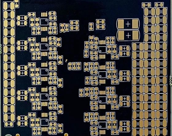
In PCB design, large areas of untreated bare copper foil should be avoided. These areas should be filled with copper pour to ensure a balanced layer structure and improve electrical performance and manufacturing stability.
Rotation Guidelines When Copper Pouring is Not Possible
If copper pouring is not possible due to design limitations, routing parameters should be set with a higher safety margin. For example, use 2 oz copper thickness and maintain a minimum spacing of 8 mil (trace-to-trace/trace-to-pad/pad-to-pad) to ensure sufficient conductivity and manufacturability.
Copper Pouring Spacing and Pattern Requirements
Copper pours should maintain an appropriate distance from functional traces and pads, preferably ≥0.5 mm, to avoid impedance coupling or manufacturing defects. Shaded (grid) copper pours, especially fine grids, are not recommended as they can cause uneven heat dissipation and increase manufacturing difficulty. Solid copper pours are preferred for improved performance and structural stability.
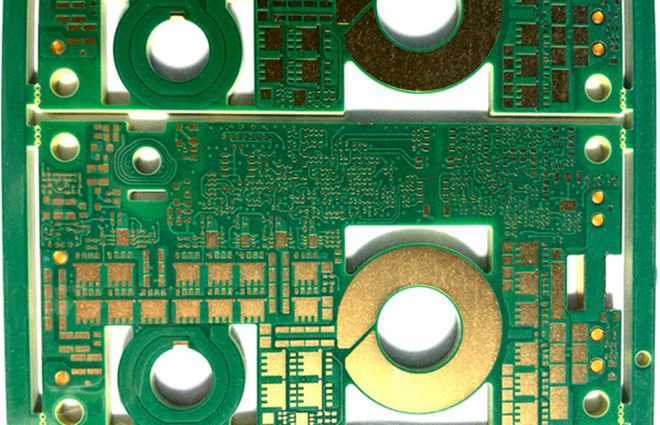
Copper Requirements for the Inner Layer of the Gold Finger Area
All inner layers containing the gold fingers must be copper-cast to prevent insufficient thickness in this area, which could reduce strength or affect insertion/removal life. Simultaneously, avoid using excessively thin stacked structures to maintain stable mechanical properties.
Copper Laying Restrictions in the Antenna Area
For PCB with wireless functionality, the copper foil layout around the antenna should be rationally handled according to the product’s antenna design requirements. Avoid arbitrarily laying copper in the antenna area to prevent negatively impacting the antenna resonant frequency, gain, or radiation efficiency.
The Importance of Copper Pour
Leaving too many unpoured copper areas on a PCB not only affects electrical performance but can also lead to manufacturing problems. Copper pouring, by covering blank areas with planar copper foil, can significantly improve the following:
Reducing grounding impedance and improving system stability
Enhancing power loop efficiency and reducing voltage drop
Shortening return paths and reducing radiation and noise
Strengthening EMC performance and improving immunity
Improving heat dissipation and structural balance, increasing board layer strength
All mainstream PCB design software supports automatic copper pouring; therefore, making copper pouring a standard design process is a key step in ensuring performance and reliability.
What are the benefits of exposed copper on a PCB?
PCB exposed copper refers to areas on a circuit board where the copper foil is intentionally left uncovered by solder mask, creating a directly accessible metal surface. This design plays several important roles in PCB manufacturing:
Enabling Electrical Connections:Exposed copper provides direct metal contact surfaces for pads, test points, etc., used for soldering component leads, continuity test probes, or grounding terminals, ensuring reliable electrical connections.
Enhancing Heat Dissipation:Copper has excellent thermal conductivity. Large areas of exposed copper help high-power devices dissipate heat more quickly, improving the overall heat dissipation efficiency of the PCB.
Improving Electromagnetic Compatibility (EMC):Exposed copper is often used to build ground planes or shielding layers, effectively reducing electromagnetic interference and improving circuit stability.
Optimizing Production Costs:In some applications, reducing the area covered by solder mask can reduce material usage and processing steps, thereby saving manufacturing costs.
Why do PCB gold fingers require copper foil?
The gold finger area is a critical location for repeated mating and plugging between the PCB and connectors, requiring strict control over thickness, tolerances, and electrical performance. Therefore, copper foil filling (copper foil casting) is necessary in the gold finger area to ensure structural and performance stability.
First, gold fingers require high consistency in board thickness. Copper foil casting in the inner layer reduces the flow space of the resin during lamination, making the board thickness easier to control and preventing failures caused by the finished product thickness approaching the lower tolerance limit.
Second, copper foil filling also improves the reliability of the manufacturing process.
Inner layer copper foil filling: Increases copper coverage, reduces resin diffusion area, and improves lamination reliability and board thickness uniformity.
Outer layer copper foil filling: Helps to distribute the electroplating current evenly, ensuring stable copper thickness on the gold finger surface, while avoiding risks such as short circuits and thinner linewidths caused by uneven electroplating and etching.
There are two common copper foil casting methods: Solid casting: Offers better current carrying capacity and shielding, but warping or copper foil detachment may occur during wave soldering. This can be mitigated by designing slots.
Shadow casting (grid): Suitable for high-frequency circuits, with good heat dissipation, but copper foil segments may create an “antenna effect” at certain frequencies, introducing EMI.
With the advancement of PCB manufacturing technology, dry film solder mask technology is now the mainstream process. In this process, grid-like copper foil is prone to copper film cracking; therefore, solid copper foil casting is recommended for the gold finger area to ensure reliability.
What causes copper exposure on a PCB?
Copper exposure on a PCB is mainly caused by two categories of reasons: intentionally exposed copper and defective exposed copper. The former is a functional requirement and is considered normal design; the latter is due to manufacturing or material issues and is considered a defect.
- Intentionally Exposed Copper
This type of exposed copper is intentionally retained by engineers during the PCB design phase for purposes such as soldering, electrical connections, testing, or heat dissipation, and is not a defect. After manufacturing, surface treatments (such as immersion gold, OSP, or plating) are usually applied to prevent oxidation.
- Intentionally exposed copper mainly includes:
1. Pad
Function: Used for soldering component leads, enabling electrical and mechanical connections.
Types: Surface mount pads, through-hole pads.
2. Test Point
Function: Used for automated testing or manual measurement, facilitating debugging and maintenance.
3. Gold Finger
Function: Used for plug-in connections, such as those on memory modules and graphics cards.
Characteristics: Generally plated with hard gold, offering high wear resistance.
4. Thermal Pad or Large Area of Bare Copper
Function: Contacts the heat dissipation surface of high-power devices, improving heat dissipation efficiency.
Design intentioned exposed copper is a normal functional requirement and part of PCB performance.
- Defective Exposed Copper
This type of exposed copper is not intentional but rather caused by damage due to production, transportation, or material issues, leading to serious risks such as short circuits, corrosion, and reduced solderability.Common causes are as follows:
1. Solder Mask Damage
Source: Damage caused by transportation compression, improper handling, mechanical contact, etc.
Risk: Exposed lines are prone to short circuits and corrosion; a typical defect.
2. Solder Mask Misalignment
Source: Misalignment occurs during solder mask exposure, exposing copper lines that should be covered.
Risk: May cause short circuits during assembly; a common process defect.
3. Insufficient Solder Mask Coverage
Source: Insufficient solder mask ink thickness or incomplete curing; often occurs in thin lines and corners.
Risk: Reduced corrosion resistance and impact on subsequent reliability.
4. Surface Treatment Layer Damage
Source: Scratches during handling, poor electroplating, chemical residue corrosion leading to plating peeling.
Risk: Copper oxidizes rapidly after exposure, making soldering difficult and increasing contact resistance.
5. Poor Raw Material Quality
For example: inferior copper foil, uneven substrate resin, poor ink adhesion.
Impact: Prone to problems such as pinholes, solder resist detachment, and exposed copper in subsequent processes.
6. Improper Manufacturing Process Control
Including: insufficient exposure, incomplete cleaning, uneven electroplating, and over-etching.
Impact: Localized copper exposure or uneven copper thickness on the finished board.
7. Improper Packaging and Transportation
Insufficient packaging protection, stacking and squeezing, and vibration and impact can all scratch the solder resist layer, leading to copper exposure.
The Impact of Copper Foil Thickness on PCB Performance
Copper foil thickness is a crucial parameter determining the electrical performance, thermal management capabilities, and overall reliability of a PCB. Different copper foil thicknesses directly affect conductivity, heat dissipation efficiency, structural strength, and manufacturing process stability. Therefore, a suitable selection must be made based on the application scenario during the design phase.
1. Impact on Electrical Performance
Thicker copper foil generally results in higher current carrying capacity and lower line resistance, effectively reducing voltage drop and heat generation in high-current or power supply lines.
Thick copper (1 oz or more): Suitable for power boards, motor drives, and power modules, providing lower impedance and higher current carrying capacity.
Thin copper (≤1 oz): Used in high-speed signals and precision control circuits, helping to control impedance and improve signal integrity.
Inappropriate copper thickness selection can lead to excessive resistance, severe heat generation, or unstable impedance, directly affecting circuit performance.
2. Impact on Heat Dissipation
Copper has excellent thermal conductivity; therefore, thicker copper foil improves the PCB’s ability to absorb and dissipate heat.
High-power devices, LED drivers, and power modules typically require thicker copper foil to aid in rapid heat dissipation and reduce localized temperature rise.
In high-density wiring, appropriately increasing copper thickness can improve overall thermal management capabilities and enhance system stability under high loads.
Insufficient heat dissipation not only affects performance but may also shorten component lifespan.
3. Impact on Mechanical Strength and Soldering Reliability
Copper foil thickness also affects pad strength, via reliability, and mechanical load-bearing capacity.
Thicker copper foil improves pad adhesion and enhances solder joint peel resistance, making it suitable for areas subjected to mechanical stress.
In solder joints subjected to significant thermal stress (such as the bottom of high-power devices), thicker copper can also reduce solder joint cracking caused by thermal expansion and contraction.
However, excessively thick copper foil can also make routing difficult and pad spacing difficult to control.
4. Impact on Manufacturing Processes
Copper foil thickness determines etching difficulty and surface finish consistency: Thicker copper makes etching more difficult, easily leading to process problems such as uneven linewidth and accelerated side etching.
Excessively thick copper foil can cause uneven electroplating, resulting in localized uneven copper areas, affecting subsequent processes such as immersion gold and tin plating.
High-thickness copper layers also place higher demands on lamination pressure and resin filling capacity.
Therefore, copper thickness design must be matched with manufacturing capabilities.
The Importance of Adding Copper Foil to PCB
In the manufacturing process of multilayer PCB, the appropriate addition of copper foil is a crucial step in ensuring product quality and structural stability. For designs with large blank areas on the board surface, failure to fill with copper foil may lead to the following problems:
Uneven or Insufficient Board Thickness: Increased resin content in blank areas can easily cause uneven thickness during lamination, affecting overall structural stability.
Uneven Electroplating Current Distribution: Insufficient local copper coverage can cause inconsistent plating thickness, leading to manufacturing defects such as linewidth variations and excessive copper etching.
Increased Risk of Warpage or Deformation: Uneven copper foil distribution can result in uneven heating, making the circuit board more prone to warpage during reflow soldering or use.
Therefore, during the manufacturing stage, Thindry adds copper foil to the inner and outer layer connectors, panel bridging areas, and the periphery of PCB units according to design requirements to balance copper distribution and improve manufacturing consistency. Simultaneously, necessary gaps are reserved at reference points, machine holes, mousebite areas, and V-cut areas to avoid affecting processing accuracy.
As a manufacturer committed to technological innovation, Thindry not only provides high-quality PCB production, but also offers one-stop PCBA services: covering high-quality PCB manufacturing, million-dollar BOM component sourcing capabilities, and professional assembly processes supported by advanced SMT equipment, helping customers complete the delivery from design to finished product more efficiently.

How to Avoid Potential Risks from Exposed Copper on PCB
While exposed copper offers significant advantages in heat dissipation, electrical performance, and structural stability, improper handling can lead to risks such as oxidation, short circuits, and poor soldering. To ensure long-term reliable PCB operation, the following measures should be taken during the design and manufacturing stages to avoid potential problems caused by exposed copper:
1. Choose Appropriate Surface Treatments
Select processes such as OSP, ENIG, and HASL based on the application to reduce copper oxidation and improve solder joint quality.
2. Control Bare Copper Area Design
Limit the area of bare copper and optimize its shape to avoid uneven etching, copper warping, or manufacturing defects.
3. Enhance Moisture Protection
Use thicker solder mask layers, conformal coatings, or local seals to reduce the risk of corrosion and short circuits caused by moisture and salt spray.
4. Optimize Pad and Wiring Spacing
Reduce electrical problems such as solder bridging and crosstalk by adding solder bridges and optimizing wiring.
5. Strict Manufacturing and Cleaning Processes
Ensure thorough cleaning and drying to prevent residual impurities from accelerating copper corrosion.
In PCB design, exposed copper is both an important means of improving performance and a potential source of reliability risks. A well-designed exposed copper layout can enhance heat dissipation, reduce impedance, and improve solder joint strength, providing stable support for high-power and high-density applications. However, improper handling can lead to quality issues such as corrosion, oxidation, and short circuits. Therefore, during design and manufacturing, it is essential to select appropriate protection methods based on process capabilities, balancing performance and risk to ensure the PCB maintains long-term stability and high reliability in practical applications.


0 Comments