
Introduction
PCB manufacturing techniques form the foundation of modern electronics production. These sophisticated and interconnected processes transform conceptual designs into the physical, functional boards that power virtually all electronic devices. A deep understanding of these techniques—encompassing design transfer, chemical etching, multi-layer lamination, precision drilling, and plating—is crucial for ensuring the performance, reliability, and yield of the final product. This article delves into the essential PCB manufacturing techniques, providing a comprehensive, step-by-step analysis of the entire fabrication workflow from initial design to final testing.
PCB Design Flow
Design is the initial step in board fabrication. It serves as the plan for PCB manufacturing and layout – the designer creates a blueprint for the PCB that fulfills all outlined requirements. The most commonly used design export software among PCB designers is a program called Extended Gerber, also known as IX274X.
Extended Gerber is an excellent PCB design software solution because it also functions in an output format. It generates all the information required by both the designer and the PCB manufacturer, such as the number of copper layers, required solder mask layers, and other component symbols. Once the PCB design blueprint is encoded by the Gerber Extended software, all different parts and aspects of the design are checked to ensure no errors are present.
After the designer completes the check, the finalized PCB design is sent to a PCB fabrication house for board construction. Upon arrival, the manufacturer checks the design in a process called Design for Manufacture (DFM) check. An effective DFM check ensures the design is manufacturable considering the capabilities of the fabrication process and does not require excessive resources or time to complete.
Progressive engineers may involve the PCB manufacturer in the DFM process during the PCB design phase, rather than waiting until the design is finalized. This allows them to make necessary changes before placing the order, saving both time and money. If critical attributes are missing from the design, it can impact the manufacturer’s ability to produce PC boards with high yield.
Printing
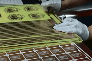
The PCB layout undergoes a unique printing process. Unlike other plans, this process requires specialized plotter printers to produce PCB films. After printing, this film is essentially the negative of the PCB itself.
The plotter prints the inner layers of the PCB using two different ink colors:
- Black ink, indicating the circuits and copper traces of the PCB.
- Clear ink, indicating the non-conductive areas of the PCB, such as the fiberglass base.
For the outer layers of the PCB design, this trend is reversed – clear ink refers to the lines of the copper pathways, while black ink also indicates areas where copper will be removed.
Each PCB layer and its accompanying solder mask have their own film, so a simple two-layer PCB requires four sheets – one for each layer and one for each accompanying solder mask.
After the films for each layer of the PCB are printed, they are aligned, and the printer uses a punch to create a hole in the films, called a registration hole. This hole serves as an alignment guide, allowing technicians to align the films throughout the manufacturing process.
Printing Inner Layer Copper
The manufacturer begins building the PCB by covering the laminate substrate with a photosensitive film called resist. The resist is made from a layer of photo-reactive chemicals that harden when exposed to ultraviolet (UV) light. The resist enables technicians to achieve a perfect match between the blueprint’s photo and the image printed onto the photoresist.
Once the resist and laminate are aligned (using the previously mentioned holes), they receive a burst of UV light.
The UV light passes through the translucent parts of the film, hardening the photoresist. This represents the copper areas that should remain as pathways. In contrast, the black ink prevents any light from reaching areas that should not harden, so they can be removed later.
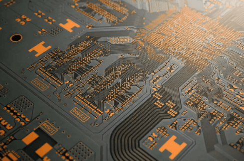
After the PCB design is printed onto a piece of laminate material, a layer of copper foil or copper coating is applied. The copper is pre-bonded to the same piece of laminate, which serves as the PCB’s foundation. The copper is then etched away to reveal the traces designed in the earlier blueprint.
The inner layers are part of the core, which consists of two copper layers with a dielectric material between them. The inner layers are treated with an etch resist to protect the copper from being etched. This treatment is done before the core undergoes the etching process. After etching, the only copper remaining is what the designer intended.
Once the board is prepared by the technicians, they wash it with an alkaline solution or use a similar process to remove any remaining photoresist. They then give it a high-pressure wash to remove any debris or particles left on the surface and let it dry. After drying, the only resist remaining on the PCB is on top of the copper. Technicians then inspect the PCB for errors.
After drying, the only resist that should remain on the PCB is on top of the copper, which remains as part of the PCB when it is eventually released. Technicians inspect the PCB to ensure there are no errors. If no errors are present, it proceeds to the next step.
Etching the Inner Layers or Core to Remove Copper
Before the PCB manufacturing process continues, the printed circuit board’s core or inner layers require the removal of excess copper. Etching involves covering the necessary copper on the board and exposing the rest of the board to chemicals. The chemical etching process removes all unprotected copper from the PCB, leaving only the amount required for the board.
The duration of this step or the amount of copper etching solvent used can vary. Larger PCBs or those with heavier structures might use more copper, resulting in more copper that must undergo etching for removal. Consequently, these boards will require additional time or solvent.
Layer Alignment
Once the technicians have cleaned each layer of the PCB, they can proceed with layer alignment and optical inspection. The registration holes mentioned earlier are used to align the inner and outer layers. To align these layers, technicians place them into a punch machine called an optical punch. The optical punch drives pins down through the holes to align the PCB’s layers.
Automated Optical Inspection (AOI)
Following optical punching, another machine performs an optical inspection to ensure no defects are present. This Automated Optical Inspection is crucial because any errors present cannot be corrected once the layers are laminated together. To confirm the absence of defects, the AOI machine compares the PCB against the Extended Gerber design, which serves as the manufacturer’s model.
After the PCB passes the optical inspection – meaning neither the technicians nor the AOI machine found any defects – it proceeds to the final few steps of PCB fabrication and production.
The AOI step is critical for the functionality of the printed circuit board. Without it, boards with potential short circuits, non-compliance with design specifications, or excess copper not removed during etching might pass through the remaining process. AOI prevents defective boards from proceeding further by acting as a quality checkpoint during production. Later, after engineers complete imaging and etching, this process is repeated for the outer layers.
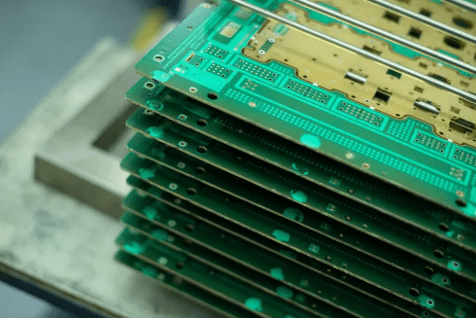
PCB Layer Lamination
The original piece of substrate is also covered in a thin copper foil, which now contains the etched copper traces. Once the outer and inner layers are ready, they can be pressed together. Dielectric material is included between the inner core and the outer layers.
These layers are clamped onto a special press table using metal clamps. Each layer is mounted on the table using dedicated pins. The technician performing the lamination process first places a layer of pre-coated epoxy resin, called prepreg, on the table’s alignment basin. From there, they build the layers in a specific sequence – copper foil, dielectric, core, dielectric, and copper foil in a four-layer “book”.
Once the copper press plate is in place, the stack is ready for pressing. The technician takes it to a mechanical press, which presses the layers down together. As part of this process, pins are punched through the laminate to ensure they are properly secured.
If the layers are secured correctly, the PCB stack is taken to the next press, the laminating press. The laminating press uses a pair of heated plates to apply heat and pressure to the laminate. The heat from the plates melts the epoxy resin inside the prepreg. Combined with the pressure from the press, this fuses the PCB layer stack together.
Once the PCB layers are laminated together, some unpacking is required. The technician needs to remove the top press plate and the pins from earlier before they can separate the actual PCB.
Drilling
Before drilling, an X-ray machine is used to locate the drill points. Then, registration holes or pilot holes are drilled so the PCB stack can be secured before more specific holes are drilled. When it’s time to drill these holes, a computer-guided drill bit makes the holes itself, using the Extended Gerber design software as a guide.
After drilling is completed, any additional copper left around the edges is filed off.
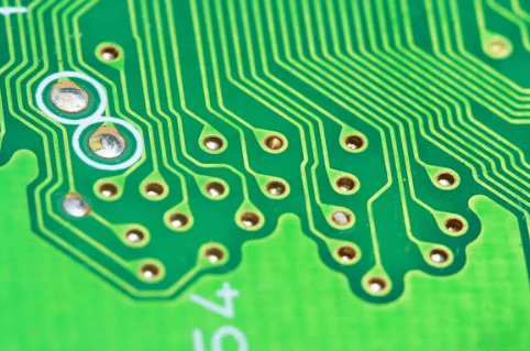
PCB Plating
After the panel is drilled, it is ready for plating. The plating process uses chemicals to fuse all the different layers of the PCB together. After a thorough cleaning, the PCB is soaked in a series of chemicals. Part of this soaking process coats the panel with a micron-thick layer of copper, which is deposited on the outermost layer and into the freshly drilled holes.
Before the holes are filled with copper, they simply expose the fiberglass substrate that makes up the panel’s interior. Soaking these holes with copper coats the walls of the previously drilled holes.
The non-conductive layers are covered with dark ink, and the copper layers are covered with light ink. This light ink allows a tin plating layer to cover and protect the copper.
Outer Layer Imaging
Earlier in the process, photoresist was applied to the PCB panel. Now it is time to apply another layer of photoresist. However, this time, the photoresist is applied only to the outer layers, as they still require imaging. Once the outer layers are coated with photoresist and imaged, they are plated in exactly the same way as the PCB’s inner layers were in the previous step. However, while the process is the same, the outer layers are plated with tin to help protect the outer layer copper.
Outer Layer Etching
In this final etching stage, the temporary tin shield helps protect the underlying copper. Using the same copper solvent as before, any unwanted copper is removed, with the tin safeguarding the valuable copper in the etched areas. After etching the outer layers, the tin shield is removed.
One of the main differences between inner and outer layer etching pertains to the areas requiring removal. Engineers remove unwanted copper and any remaining resist coating during the etching process, preparing the outer layers for AOI and solder masking, in what is known as a subtractive process.
Outer Layer AOI
Similar to the inner layers, the outer layers typically undergo an Automated Optical Inspection (AOI). This optical inspection ensures the layer meets the design’s exact requirements. It also verifies that the previous step removed all excess copper from the layer, resulting in a functional printed circuit board without incorrect electrical connections.
Solder Mask Application
Before applying the solder mask, the panel requires thorough cleaning. Then, the solder mask is applied via screening or curtain coating and dispensed for UV curing. The PCB undergoes a visual inspection, which is a critical element of this setup, as many Original Equipment Manufacturers (OEMs) do not permit solder mask repairs. If solder mask voids or inconsistencies exist, the solder mask can be stripped and the process restarted.
If the solder mask passes inspection smoothly, it is baked and cured. This mask provides additional protection for the board’s copper against damage from corrosion and oxidation. Next, ultraviolet light is directed onto the board, indicating where to remove the solder mask. This process is referred to as “Liquid Photoimageable” solder mask application.
Silkscreen Application and Surface Finish Application
Since the PCB requires information to be displayed directly on the board, the manufacturer must print important data onto the board surface in a process called silkscreen application, nomenclature, or legend printing. This information includes the following:
- Company ID number
- Warning labels
- Manufacturer marks or logos
- Part number
- Pin locators and similar markings
- Component designators, polarity markers, and connector pinouts
After the aforementioned information is printed onto the printed circuit board, typically using an inkjet printer, the PCB undergoes surface finish application. They then proceed to the testing, cutting, and inspection stages. For clarity, 8-point font and smaller silkscreen text require laser printing.
Finishing the PCB
Completing the PCB involves plating conductive materials, such as:
- Immersion Silver: This plating option offers low signal loss, but the finish may oxidize and tarnish. It is lead-free and complies with Restriction of Hazardous Substances (RoHS) standards.
- Hard Gold: Gold is one of the more expensive plating alternatives, but it is durable, RoHS compliant, and lead-free. It is commonly used for gold fingers where daughterboards are inserted into the motherboard multiple times.
- Electroless Nickel Immersion Gold (ENIG): ENIG is one of the most common PCB surface finishes. It is more expensive than some options but cheaper than gold. It is known for its superior service life and durability. It is also RoHS compliant and provides better component pad flatness and coplanarity.
- Hot Air Solder Leveling (HASL): HASL is a cost-effective, long-lasting solution with the added advantage of reworkability. However, it contains lead and does not meet RoHS compliance standards.
- Lead-Free HASL: Removing lead from HASL maintains its cost-effectiveness and reworkability advantages while making it RoHS compliant. Both types of HASL are only effective for 20-mil pitch components, whereas 16-mil pitch components require alternative coatings to ensure component pad flatness and coplanarity.
- Immersion Tin (ISn): This option is popular in press-fit applications and is RoHS compliant with tight hole tolerances. However, using this medium can lead to soldering issues like tin whiskers. It also has a short shelf life of approximately 3-6 months. These PCBs must be packaged and stored to prevent exposure to free-flowing air and contained in temperature- and humidity-controlled environments.
- Organic Solderability Preservative (OSP): OSP is RoHS compliant and cost-effective but has a shelf life of 6-11 months.
- Electroless Nickel Electroless Palladium Immersion Gold (ENEPIG): This option requires careful handling for proper performance. It features high solder joint strength, and the palladium coating post-plating helps prevent nickel corrosion. However, it is less cost-effective than other options.
The correct material depends on design specifications and the customer’s budget. However, applying this finish creates an essential characteristic for the PCB. The finish allows assemblers to mount electronic components. The metal also covers the copper to protect it from oxidation that can occur upon exposure to air.
Electrical Reliability Testing
After coating and curing where necessary, technicians subject the PCB to a series of electrical tests. Electrical testing must adhere to the standards of IPC-9252, the Guidelines and Requirements for Electrical Testing of Unpopulated Printed Boards. The primary tests performed are circuit continuity and isolation tests. The circuit continuity test checks for any breaks, known as “opens,” within the PCB. The circuit isolation test checks the isolation value of various parts of the PCB to check for any short circuits.
While electrical tests are primarily for ensuring functionality, they also serve to test how well the initial PCB design has withstood the manufacturing process.
In addition to basic electrical reliability tests, other tests are available to determine if the PCB is functioning correctly. One of the main tests used to do this is called the “bed of nails” test. In this, several spring-loaded fixtures are attached to test points on the circuit board. The spring-loaded fixtures then apply pressure up to 200g to the test points on the board to observe the PCB’s ability to withstand high-pressure contact at its test points.
If the PCB has passed the electrical reliability tests and any other tests the manufacturer chooses to implement, it can proceed to the next step: routing and inspection.
Profiling and Routing Output
Profiling requires the manufacturing engineer to identify the shape and dimensions of the individual printed circuits to be cut from the construction panel. This information is typically located in the design’s Gerber files. This profiling step guides the routing process by programming where the machine should create scores on the construction panel.
Routing or scoring makes it easier to separate the boards. A router or CNC machine creates several small tabs along the edges of the boards. These tabs allow the boards to be snapped off quickly without damage. However, some manufacturers may opt to use V-scoring instead. The machine will create V-shaped cuts along the sides of the boards.
PCB manufacturers sometimes use a hard tool punch to separate the PCB from the manufacturing panel. However, this is typically only done in high-volume applications. Other times, break-away tabs used in customer array designs allow the assembler to remove individual boards after PCB assembly.
Quality Check and Visual Inspection
After the boards are scored and separated, the PCB must undergo one final inspection before packaging and shipping. The final inspection verifies several aspects of the board’s construction:
- Hole Location and Tolerances: The PCB’s hole sizes must match across all layers and meet design requirements.
- Board Dimensions: The PCB’s dimensions must align with the original design specifications.
- Cleanliness: The manufacturer must ensure the board is free of dust, debris, and unwanted particles.
- Finish: The finished board must have smooth edges, free of burrs or sharp areas.
- Electrical Reliability: Any board that failed electrical reliability tests must have been sent back for rework and retesting.
Packaging and Delivery
The final stage of PCB manufacturing is packaging and delivery. Packaging typically involves materials that seal around the printed circuit board to prevent dust and other foreign matter from entering, similar to vacuum sealing. The sealed boards then go into containers to protect them from damage during transit. Finally, they are sent out for delivery to the customer. Depending on the customer’s specifications, packaging with Electrostatic Discharge (ESD) protection may be used.
Summary
The fabrication of a Printed Circuit Board is a testament to precision engineering, where a suite of complex PCB manufacturing techniques converge to create a reliable electronic foundation. As analyzed, the entire workflow underscores the critical importance of Design for Manufacturability (DFM) in bridging the design intent with production realities. Core techniques such as imaging and etching, layer-to-layer registration during lamination, and controlled plating processes are pivotal in determining the board’s electrical and mechanical characteristics. Furthermore, rigorous quality control techniques, primarily Automated Optical Inspection (AOI) and electrical testing, are non-negotiable for ensuring functionality and reliability. Ultimately, the selection of final techniques, such as the application of surface finishes, involves a critical balance between performance, cost, and application requirements. Mastery of these interconnected PCB manufacturing techniques is fundamental to advancing electronic design and achieving manufacturing excellence.


0 Comments