
Introduction
The Printed Circuit Board Assembly (PCBA) process is a critical series of precise and interconnected steps that transform a bare board and electronic components into a fully functional circuit assembly. This intricate process, commonly known as the PCB Assembly Process, is foundational to modern electronics manufacturing, bridging the gap between design and a tangible, operational product.
A successful outcome hinges on a meticulously controlled sequence—from initial design verification and component sourcing to automated placement, soldering, and rigorous testing. Each phase, whether automated or manual, must be executed with precision to ensure the final product meets all specified quality, reliability, and performance standards. Ultimately, the integrity of the entire electronic device depends on the excellence of its PCB Assembly Process.
Step-by-Step PCB Assembly Process
Let’s explore the detailed steps involved in the PCB assembly process. Each step plays a vital role in creating a high-quality, fully functional printed circuit board.
DFA: Verification of Gerber/ODB++ and BOM
The PCB assembly process begins with Design for Assembly (DFA) verification. This critical step involves reviewing the Gerber files or ODB++ data, which contain PCB design information, along with the Bill of Materials (BOM).
- Gerber File Verification: Gerber files are the standard format for PCB design data. They include information on board layers, component placement, and other key details. The verification process ensures these files are accurate and complete.
- ODB++ Data Inspection: ODB++ is a more comprehensive PCB data exchange format that includes both design and manufacturing information. If ODB++ is used instead of Gerber files, it is thoroughly validated.
- BOM Verification: The Bill of Materials lists all components required for PCB assembly. This step ensures all components are correctly specified and available for the assembly process.
DFA verification is essential as it helps identify any potential issues in the design or component specifications before physical assembly begins, saving time and resources in the long run.
PCB Fabrication
Once the design is verified, the next step is PCB fabrication. This process involves creating the bare PCB, which will serve as the foundation for component assembly.
- Material Selection: The process begins with selecting a suitable substrate, typically a glass-epoxy material with copper layers.
- Imaging: The PCB design is transferred onto the copper layer using photolithography.
- Etching: Excess copper is removed, leaving only the desired circuit pattern.
- Drilling: Holes are drilled for through-hole components and vias.
- Plating: The board is plated with additional copper to ensure reliable connections.
- Solder Mask and Silkscreen: A solder mask is applied to protect the copper traces, and a silkscreen is added for component labels and other markings.
The outcome of this step is a bare PCB ready for component assembly.
Incoming Quality Control (IQC)
Before assembly begins, all incoming materials, including the fabricated PCBs and electronic components, undergo rigorous quality control inspections.
- PCB Inspection: Bare PCBs are examined for defects such as scratches, dents, or incorrect hole sizes.
- Component Verification: All electronic components are verified against the BOM to ensure they meet required specifications.
- Visual and Functional Testing: Components may undergo visual inspection and basic functional testing to confirm they are undamaged and operate correctly.
This step is crucial for detecting any defects or discrepancies early, preventing potential issues during assembly or in the final product.
Machine Programming – Gerber/CAD to Centroid/Placement/XY Files
Prior to physical assembly, the assembly machines must be programmed with accurate component placement information.
- Data Conversion: Gerber or CAD files are converted into formats understandable by assembly machines, typically centroid or XY files.
- Placement Programming: Machines are programmed with precise coordinates for where each component should be placed on the PCB.
- Component Feeder Setup: Component feeders, which supply parts to the placement machine, are configured according to the programming.
This step ensures the automated assembly process places components accurately and efficiently.
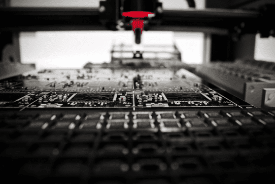
SMT Assembly Process Using a Pick-and-Place Machine
Surface Mount Technology (SMT) is a method for producing electronic circuits where components are mounted directly onto the PCB surface. This process involves several sub-steps:
a. Solder Paste Stenciling
- A stencil is aligned with the PCB.
- Solder paste is applied over the stencil, depositing it onto the board’s pads.
- The stencil is removed, leaving precise amounts of solder paste on the pads.
b. SMT Component Placement
- The PCB is loaded into a pick-and-place machine.
- The machine uses vacuum nozzles to pick up SMT components from feeders.
- Components are accurately placed in their designated positions on the PCB.
c. Pre-Reflow Automated Optical Inspection (AOI)
- An AOI machine scans the board to verify correct component placement and orientation.
- Any issues detected at this stage can be corrected before soldering.
d. Reflow Soldering
- The PCB passes through a reflow oven with carefully controlled temperature zones.
- The solder paste melts and then cools, forming solid solder joints between the components and the PCB.
e. Post-Reflow Automated Optical Inspection (AOI)
- Another AOI is performed to inspect solder joint quality and ensure no components shifted during reflow.
f. X-Ray Inspection
- For complex components like Ball Grid Arrays (BGAs), X-ray inspection is used to examine solder joints that are not visible from the surface.
g. Wave Soldering
- Although primarily used for through-hole components, wave soldering can also be applied to SMT components on the bottom side of the board.
- The PCB passes over a wave of molten solder, which adheres to exposed metal areas.
h. Flying Probe Test (FPT)
- This is an automated electrical test that checks for shorts, opens, and component values.
- It is particularly useful for low-volume or prototype boards where creating a dedicated test fixture is not cost-effective.
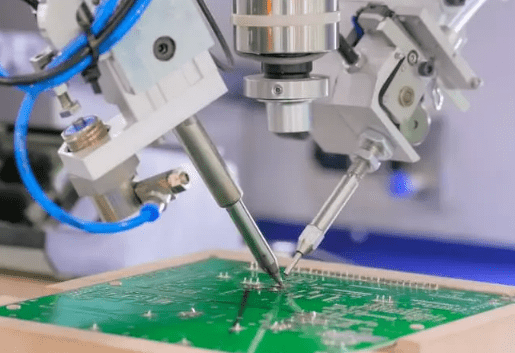
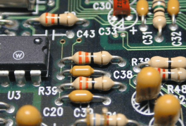
Through-Hole Assembly
While SMT is prevalent in modern electronics, through-hole assembly is still used for certain components and specific applications.
- Components are inserted into pre-drilled holes on the PCB.
- The component leads protrude to the opposite side of the board.
- These leads are then soldered, typically using wave soldering or selective soldering techniques.
Through-hole assembly is usually performed after SMT and is often a more manual process.
Cleaning of the Assembled Board
After soldering, the PCB is cleaned to remove any flux residues or other contaminants.
- Cleaning methods may include solvents, aqueous solutions, or even ultrasonic cleaning for more stubborn residues.
- Proper cleaning ensures the long-term reliability of the PCB by preventing corrosion and other issues caused by residues.
Soldering of Non-Cleanable Components
Some components are sensitive to cleaning processes and must be soldered after the cleaning step.
- These components are typically hand-soldered by skilled technicians.
- Special care is taken to ensure these components are not exposed to any cleaning agents that could damage them.
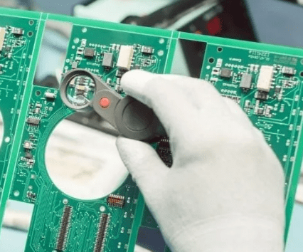
Final Inspection and Testing
Once assembly is complete, the PCB undergoes final inspection and testing to ensure it meets all quality and functional requirements.
- Visual inspection is conducted to check for any obvious defects.
- Functional testing verifies that the PCB operates as intended.
- In-Circuit Test (ICT) or Flying Probe Test may be used to inspect individual components and connections.
- Burn-in testing may be performed for critical applications to ensure reliability.
Conformal Coating
For PCBs that will be exposed to harsh environments, a conformal coating may be applied.
- This polymer film protects the PCB and its components from moisture, dust, and chemicals.
- The coating can be applied by dipping, spraying, or brushing, depending on the board and requirements.
Packaging and Shipping
The final step in the PCB assembly process is packaging and shipping.
- Assembled PCBs are carefully packaged to protect them from electrostatic discharge and physical damage.
- Appropriate labeling and documentation are included with the shipment.
- The PCBs are then shipped to the customer or proceed to the next stage of product assembly.
Summary
The PCB assembly journey, from file verification to final shipment, is a testament to engineering precision and process control. By rigorously adhering to this detailed sequence—encompassing DFA, IQC, automated assembly, and multiple inspection points—manufacturers can achieve high first-pass yields and ensure end-product reliability. A robust PCBA process is therefore not merely a production checklist, but a fundamental pillar for building trustworthy and successful electronic products.


0 Comments