
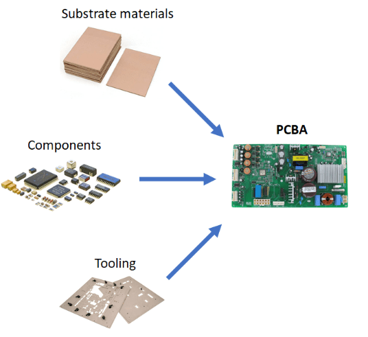
The PCBA (Printed Circuit Board Assembly) manufacturing process encompasses a series of stages including PCB fabrication, component procurement and inspection, SMD placement, DIP packaging, programming, testing, and aging. An excessively long supply and manufacturing chain can lead to a high incidence of PCBA board failures.
However, quality control within the PCBA process can effectively mitigate the majority of these failures. Consequently, most professional PCBA assembly manufacturers implement a robust quality control system for their PCBA processes to ensure the quality of their PCBA assembly services. Establishing such a system is paramount for any PCB assembly enterprise. This article will elucidate several key methods for quality control in PCBA processes.
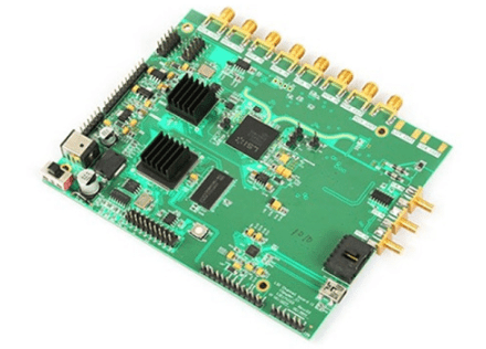
PCBA Manufacturing
Upon receiving a PCBA order, convening a pre-production meeting is particularly crucial. This meeting primarily involves a technical analysis of the PCB Gerber files and the submission of a Design for Manufacturability (DFM) report based on specific customer requirements. Many small-scale manufacturers often overlook this step, leading to subsequent complications. Another critical task in PCBA manufacturing is the inspection of the PCB design. As the foundation of PCB assembly, the PCB design fundamentally determines the quality of the PCBA build. A poor PCB design not only predisposes the board to quality issues but also results in significant rework and repair efforts.
Incoming Material Inspection (IMI)
This is the first line of defense in quality control, preventing defective materials from entering the production line.
- PCB Inspection:
- Visual Check: Inspection for scratches, dents, copper foil blistering, solder mask imperfections, warping, etc.
- Dimensional Check: Using calipers or optical Coordinate Measuring Machines (CMMs) to verify that outline dimensions, hole diameters, and hole positions conform to the Gerber file specifications.
- Solderability: Conducting solderability tests when necessary to assess the oxidation status of pad surfaces (e.g., ENIG, HASL).
- Component Inspection:
- Visual Check: Inspection for pin oxidation, deformation, and the clarity and accuracy of markings.
- Electrical Performance: Sampling key components like resistors and capacitors to verify their values are within specified tolerance ranges.
- Solderability: Performing solderability tests on critical components such as ICs and connectors.
- Solder Paste Inspection:
- Brand & Specification: Confirming the use of the specified brand and type (e.g., lead-free, leaded, particle size).
- Storage & Thawing: Checking adherence to refrigeration and thawing requirements to prevent moisture absorption.
- Viscosity Test: Regularly using a viscometer to check the solder paste’s viscosity, ensuring it is suitable for printing.
In-Process Quality Control
This is the core of quality control, focusing on maintaining quality at each process step by controlling key parameters.
- Solder Paste Printing
- Stencil Inspection: Ensuring stencil aperture sizes are correct, unobstructed, and with sufficient tension.
- Printing Parameter Control:
- Squeegee: Pressure, speed, and angle.
- Separation: Speed and distance.
- Real-time Monitoring & Inspection:
-
- SPI (Solder Paste Inspection): A standard feature in modern PCBA lines. The SPI machine utilizes 3D optical scanning to precisely measure the volume, area, height, and shape of the solder paste on pads post-printing. It promptly detects defects such as insufficient solder, excess solder, scooping, misalignment, and bridging, feeding data back to the printer for parameter adjustment, enabling closed-loop control.
- Component Placement
- Feeder Setup Verification: Implementing a “two-operator” verification system or barcode scanning to ensure the reel on the feeder matches the programmed Bill of Materials (BOM), preventing wrong, misplaced, or reversed components.
- Placement Accuracy Control:
- First Article Inspection (FAI): A comprehensive check of the first assembled board before mass production, verifying the position, polarity, and part number of all components.
- Vision System: The high-precision cameras on the placement machine identify component fiducials, pins, and polarity to correct placement positions.
- Placement Defect Rate Monitoring: Real-time monitoring of the placement machine’s component discard rate; a high rate indicates potential issues with nozzles, vacuum, or feeders.
- Reflow Soldering
- Reflow Profile Testing: This is critical for soldering quality.
-
- Method: Using a profiler and thermocouples to measure temperatures at key points on a production board.
- Key Parameters: Ramp-up rate in the preheat zone, temperature and duration in the soak zone, peak temperature and time above liquidus (TAL) in the reflow zone, and cooling rate. These must be set and periodically validated based on the solder paste and PCB/component specifications.
- Nitrogen Atmosphere: For high-reliability products (e.g., those with BGAs or fine-pitch components), introducing nitrogen into the reflow oven reduces oxidation and enhances solder joint quality.
- Post-Reflow Inspection: Boards undergo a preliminary visual inspection post-soldering to quickly identify gross defects like solder bridges, cold joints, or tombstoning.
- Wave Soldering (if applicable)
- Flux Application: Controlling the uniformity of the spray flux quantity.
- Wave Soldering Temperature Profile: Requires similar testing and monitoring of preheat and soldering temperatures.
- Wave Dynamics & Conveyor Speed: Ensuring proper solder wetting for through-hole component leads.
Post-Soldering Inspection and Testing
This stage provides the final validation of the outcomes from all preceding processes.
- Automated Optical Inspection (AOI)
- Function: AOI uses high-resolution cameras to capture images of the PCBA from various angles and compares them to pre-programmed standard images.
- Detectable Defects: Missing, wrong, or reversed components; component misalignment, lift-off; solder bridges, insufficient solder, solder balls, tombstoning, etc.
- Location: Can be placed after reflow soldering, after wave soldering, or before final testing.
- X-Ray Inspection (AXI)
- Function: Essential for inspecting hidden solder joints, such as those under Bottom-Termination Components like BGA, CSP, QFN, and for assessing the internal fill of through-hole joints, where AOI is ineffective.
- Detectable Defects: Voids (bubbles) in BGA solder joints, bridging, insufficient solder, non-wetting, and inconsistent solder ball size.
- In-Circuit Test (ICT) / Flying Probe Test
- ICT: Uses a custom bed-of-nails fixture to make contact with test points on the PCBA, performing electrical tests. It can detect opens, shorts, resistor/capacitor values, etc., but involves high fixture costs.
- Flying Probe Test: Utilizes 2-8 movable probes for testing, eliminating the need for expensive custom fixtures. Ideal for low-volume, high-mix production.
- Functional Test (FCT)
- Function: Simulates the end-use environment of the product by powering up the PCBA and testing all or part of its functionalities. This is the most direct and user-relevant test.
- Forms: Can range from a simple power-on test to complex procedures involving firmware programming, running test scripts, and verifying input/output signals.
Management and Process Control
- Electrostatic Discharge (ESD) Protection: The entire workshop must adhere to ESD standards, with operators wearing grounded wrist straps and using ESD-safe workstations and flooring to prevent damage to sensitive components.
- Traceability System: Utilizing barcodes or QR codes to record the material batches, equipment, operators, and process parameters (e.g., reflow profile) for each PCBA. This enables rapid traceability and isolation in case of defects, facilitating precise quality control.
- First Article, In-Process, and Last Article Inspection:
- FAI: Comprehensive verification before batch production starts.
- In-Process Audit: Periodic checks by quality personnel on the production line to monitor process status and product consistency.
- Last Article Inspection: Comparing the first and last units of a batch to assess production process stability.
- Continuous Improvement (CI): Employing Statistical Process Control (SPC) to analyze data collected from SPI, AOI, and ICT equipment, monitoring long-term process capability trends (e.g., Cp/Cpk values), identifying variations, and driving root cause analysis and process optimization.
In-Depth and Advanced Quality Control Methods
- Quality Control at the Design Stage: Prevention at Source
Quality is built in during design, not just inspected in later. DFM/DFA/DFT are crucial in PCBA. - Advanced Inspection and Testing Technologies
- 3D AOI and 3D SPI: Compared to 2D, 3D technology provides more accurate measurement of component height/coplanarity and absolute solder paste volume, significantly improving detection accuracy and reducing false calls.
- Automated X-Ray Inspection (AXI): Used not only for sampling but also for 100% inline inspection of critical assemblies (e.g., all BGAs in automotive electronics). AXI, combined with software algorithms, can automatically judge BGA solder ball shape, size, spacing, and internal voiding against IPC standards.
- Boundary Scan Test (JTAG): Primarily used for testing interconnects on digital and mixed-signal ICs. It utilizes the built-in JTAG (IEEE 1149.1) port of ICs to test pin-to-pin connections (opens/shorts) via a simple 4/5-wire interface, and can perform basic functional tests on some ICs. It is particularly effective for high-density boards with limited test access.
- Destructive Physical Analysis (DPA) and Reliability Testing
These are typically used for first-article qualification, new process validation, or periodic quality audits.- Cross-Sectioning (Microsection Analysis): A specific location on the PCBA (e.g., a BGA solder joint, plated through-hole) is potted in epoxy, then ground, polished, and examined under a metallurgical microscope. This “gold standard” method assesses IMC layer thickness, solder joint grain structure, plating quality, and detects micro-defects like cracks or blowholes.
- Dye and Pry Test: Used to detect cracks in BGA solder joints. Dye is penetrated under the BGA, allowed to cure, then the BGA is pried off. The dye pattern on the fractured surfaces reveals the presence and extent of cracks under a microscope.
- Thermal Cycling/Shock Testing: Subjecting PCBA to hundreds or thousands of cycles in an environmental chamber simulates real-world temperature variations over the product’s lifetime. Subsequent functional testing and cross-sectioning assess long-term reliability and solder joint fatigue resistance.
- Vibration and Mechanical Shock Testing: For automotive, aerospace, or portable devices, these tests simulate vibration and shock environments during transport and use, verifying the mechanical integrity of solder joints and components.
- Data-Driven Intelligent Quality Control
This embodies Industry 4.0 principles in the PCBA domain.- Manufacturing Execution System (MES): The MES acts as the “brain” of the production line, enabling full digital traceability. Each board’s serial number can be linked to all its production data: solder paste batch, placement program, reflow profile, test results, etc.
- Statistical Process Control (SPC): SPC is integrated in real-time with SPI, AOI, etc. The system automatically generates control charts for key parameters (e.g., solder paste volume, component placement offset). It triggers alerts when data shows abnormal trends, enabling predictive intervention before non-conforming products are made.
- AI and Machine Learning in AOI/SPI:
- Traditional AOI: Relies on manually set strict thresholds, often causing high false call rates, requiring manual review and reducing efficiency.
- AI-powered AOI: Employs deep learning algorithms to “train” the machine on millions of images of good and defective boards. It not only identifies true defects more accurately but also learns to accept harmless, natural variations in appearance (e.g., different flux residue patterns), drastically reducing false calls and improving inspection efficiency and accuracy.
- Supplier and Supply Chain Management
- Supplier Audit and Qualification: Conducting rigorous on-site audits of key component (e.g., BGA, CPU) and PCB suppliers to assess their quality systems, process capability, and stability.
- Joint Quality Improvement: Establishing data-sharing mechanisms with core suppliers to collaboratively analyze the root causes of incoming material defects and drive continuous improvement.
Summary
The Evolution from Quality Control to Quality Assurance
Modern PCBA quality management has evolved from an isolated, inspection-centric “Quality Control” phase to a comprehensive “Quality Assurance” system that spans the entire product lifecycle, with a core focus on prevention.
- Proactive Prevention: Through DFX, supplier management, and process qualification.
- In-Process Control: Via real-time monitoring and closed-loop feedback using SPI, AOI, and X-Ray.
- Post-Process Verification & Traceability: Through ICT, FCT, and full data traceability via MES.
- Continuous Improvement: Leveraging SPC, big data, and AI analytics to drive ongoing process and quality enhancement.
This integrated system tightly couples technology, processes, and personnel to collectively ensure the high quality, reliability, and yield of PCBA products.


0 Comments