




If you are preparing to order your first board, here is a practical guide to what prototyping actually involves, the design traps that catch beginners, and how to get working hardware on your desk with the fewest iterations possible.
You spend nights routing traces, checking connections, and running Design Rule Checks (DRC) in your CAD tool. The software shows green lights across the board. You export your design files, send them to the fabricator, and wait.
A few days later, the package arrives. You open it, grab your soldering iron, and immediately run into a wall: a microcontroller footprint is slightly too small because you misread a datasheet pitch, or a trace runs so close to a mounting hole that the screw head scrapes off the solder mask and shorts the board.
This is the reality of hardware development. A prototype is not a failed final product; it is a sanity check. Its job is to expose design flaws when they cost 50 USD to fix, rather than 5000 USD during a high-volume production run.
What is a PCB Prototype, Really?
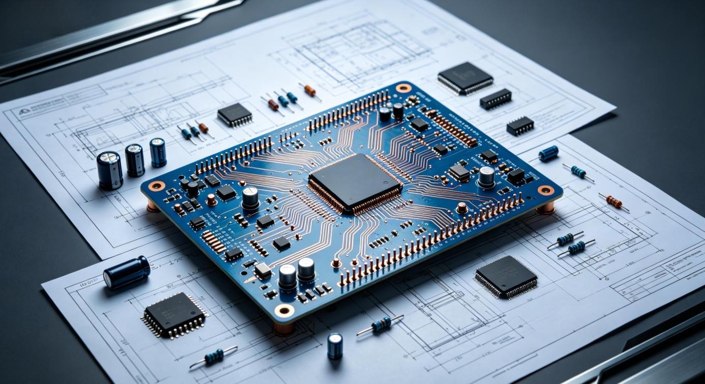
In theory, a prototype is a small batch of boards (usually $5 to $10 pieces) used to test form, fit, and function before committing to volume production.
In the real world, pcb prototyping is all about compromise. To keep costs low and turnaround times fast, manufacturers group multiple designs from different customers onto large panels (a process called “panelization” or “pooling”). Because these designs share the same fabrication run, you must design within standard parameters.
Understanding this explains why choosing non-standard board thicknesses, unusual solder mask colors, or heavy copper weights suddenly adds days to your lead time and dollars to your invoice. If your design doesn’t absolutely require exotic materials, sticking to the standard offering is always the smartest move for your budget.
8 Design Pitfalls That Stop Production
When files arrive at a manufacturing plant, engineers run a Design for Manufacturability (DFM) review. Here are the most common issues that trigger support tickets, delay prototype runs, or yield non-functional hardware:
1. The Annular Ring Violation
When a drill bit passes through a via pad, it needs to hit the dead center. In the physical world, drills drift slightly due to mechanical tolerances. The “annular ring” is the ring of copper left around the drilled hole.
If your via pads are too small, a slight drill drift will cut the trace connection entirely, leading to open circuits.
The Fix: For standard prototypes, keep your minimum single-side annular ring width (). Since the pad diameter , drill hole diameter , and ring width relate by , if your drill is , your pad diameter must be at least .
2. Silkscreen Overlapping Pads
Solder mask keeps solder on the pads; silkscreen identifies where components go. Solder will not adhere to silkscreen ink. If a component label, logo, or boundary line overlaps a copper pad, you will end up with weak joints, tombstoning, or total assembly failures.
The Fix: Do not rely on the factory to automatically trim your overlapping silkscreen. Run a silkscreen clearance check in your CAD software and keep text and lines at least away from any exposed copper pads.
3. Missing Thermal Reliefs on Planes
If you connect a component pad directly to a massive copper ground plane, that plane acts as a heatsink. When you touch your soldering iron to the pad, the heat dissipates into the plane instantly. The solder won’t melt properly, resulting in a cold joint.
The Fix: Use thermal relief connections (spokes) for pads connected to planes. This restricts heat flow during soldering while maintaining electrical connection.
   Solid Connection (Hard to Solder)      Thermal Relief (Easy to Solder)
          [  PAD  ]                                         \    [  PAD  ]  /
        #############                            -[#  PAD  ]-
        # GND PLANE #                              /    [  PAD  ]  \
        #############                           ###############
4. Footprint Sizing & Pitch Mismatch
Component packages can be deceptive. A “” resistor in metric () is vastly different from an imperial “” (, which is metric , or ). Pin pitches on ICs can also vary by fractions of a millimeter between different manufacturer variants (e.g., SOIC vs. TSSOP).
The Fix: Print your PCB design on paper at a 1:1 scale. Place your physical components directly onto the paper to verify that the footprints match the actual hardware before ordering.
5. Acid Traps (Acute Angle Traces)
When routing traces, joining them at acute angles (less than 90∘) creates a pocket. During the chemical etching process, the acid solution gets trapped in these tight corners and cannot be washed away easily. Over time, the trapped acid over-etches the copper, causing the trace to narrow or break completely.
The Fix: Although modern alkaline etching has reduced this risk, it is still best practice to avoid routing traces at sharp angles. Keep corners at 135∘ (45-degree routing) or use smooth curves to prevent chemical entrapment and signal reflection.
6. Copper Slivers (Narrow Copper Flaps)
Copper slivers occur when very narrow strips of copper are left on the board, often during the generation of copper pours. During manufacturing, these tiny, fragile slivers can peel off the board, float around in the chemical baths, and land back on the board—causing random short circuits that are incredibly hard to debug.
The Fix: Set your copper pour fill rules to remove “dead copper” and ensure the minimum copper width is at least 0.2 mm ().
7. Traces Too Close to the Board Edge
When the factory cuts your boards out of the panel using V-scoring or routing, the cutting tool has a mechanical tolerance. If you route traces or place copper pours right up to the board outline, the cutting blade can expose or shear the copper, leading to corrosion or short circuits against metal enclosures.
The Fix: Maintain a clearance of at least 0.3 mm (1) between any copper features and the board outline. For V-scored edges, increase this to 0.5 mm ().
8. Poor Decoupling Capacitor Placement
This is a functional failure rather than a manufacturing one. Decoupling (bypass) capacitors are designed to suppress high-frequency noise from entering the IC. If you place the capacitor far away from the power pin, the trace inductance defeats the purpose of the capacitor, causing erratic system resets or EMI issues.
The Fix: Always place decoupling capacitors as close as physically possible to the power pin of the IC, ensuring the connection trace goes directly from the capacitor pad to the pin before connecting to the power plane.
The “Standard Spec” Formula for Fast, Cheap Prototyping
If you want your prototype quickly and without extra fees, stick to the industry-standard baseline. Deviating from these specs requires custom setups at the factory.
| Parameter | Standard Choice (Fastest & Cheapest) | Why? |
|---|---|---|
| Layer Count | 2 Layers | Easiest to manufacture and test. |
| Material | Standard FR-4 (Tg 130-140) | The baseline fiberglass board material. |
| Board Thickness | 1.6 mm | The global standard; panels are always in stock. |
| Copper Weight | 1 oz (35 μm) | Perfect for signals and low-to-medium power. |
| Solder Mask | Green | Green masks cure faster and allow the easiest visual inspection. |
| Surface Finish | HASL (Lead-free) | Inexpensive, durable, and easy to hand-solder. |
| Trace/Space | 6 mil/6 mil () | Easily produced without high-precision tooling. |
Only upgrade to 4 layers, ENIG (Gold) finish, or thin boards (like 0.8mm) if your design specifically demands it—such as for high-speed signals, BGA packages, or tight mechanical enclosures.
Sourcing the Handoff Package
When you click order, you need to provide a complete dataset. A missing file means your order sits in a queue while customer service tries to reach you.
Here is what a complete fabrication and assembly package looks like:
For Bare PCB Fabrication:
- Gerber Files (RS-274X or X2 format): A set of files representing each layer (Top/Bottom Copper, Solder Mask, Silkscreen, Board Outline).
- Drill Files (Excellon format): Coordinates and sizes for all holes.
For PCB Assembly (PCBA):
- Bill of Materials (BOM): A spreadsheet detailing every part. It must include the Manufacturer Part Number (MPN), quantity, and reference designators (e.g., C1, R5). Generic descriptions like “10k resistor” will delay sourcing; specify the exact tolerance, package size, and manufacturer.
- Pick-and-Place File (Centroid/XY File): A text file containing the X/Y coordinates, rotation, and layer (Top/Bottom) for every component so assembly machines know where to place them.
Why Turnkey Prototyping is Replacing DIY Sourcing
Historically, engineers ordered bare boards, ordered components from distributors, and spent hours hand-soldering prototypes under a microscope.
Today, many developers opt for Turnkey PCB Assembly. This means the PCB fabricator handles the board manufacturing, sources the components directly from authorized distributors, and runs the boards through an SMT (Surface Mount Technology) assembly line.
Why go turnkey for just 5 boards?
- Component Sourcing Accuracy: Sourcing parts from different vendors introduces shipping delays and the risk of ordering the wrong package variant. A turnkey service centralizes this process.
- Professional SMT Soldering: Hand-soldering QFNs, BGAs, or 0201 capacitors is difficult and prone to bridging. Automated assembly ensures clean connections.
- Unified Accountability: If a board doesn’t work, you don’t have to figure out if it was a fabrication defect, a bad component, or a manual soldering error. The single vendor is responsible for delivering a completed, inspected assembly.
Prototyping is a cycle. By avoiding common layout errors, staying within standard factory parameters, and providing clean documentation, you can turn your design concepts into working, physical hardware on the very first try.



0 Comments