
If you want a board that works in production, you need to design for PCB from the start. Not after routing. Not after the first failed build. The earlier you make the right decisions, the less you pay later.
A PCB is not only an electrical object. It is a manufacturing object. It must be fabricated, assembled, tested, and shipped. If the design ignores that, the cost shows up fast. Rework. Delay. Scrap. Field failures.
This is why design for PCB matters. It is the difference between a clean release and a painful correction cycle.
What Does Design for PCB Mean?
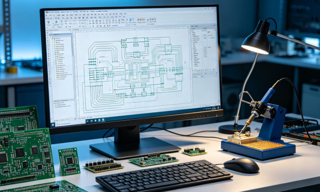
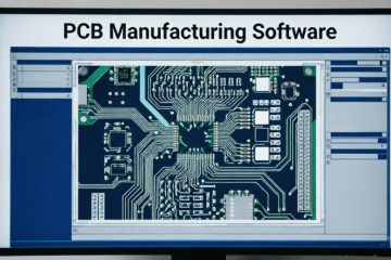
Design for PCB refers to the process of creating a printed circuit board layout that turns an electronic circuit into a manufacturable board. It includes schematic design, component placement, routing, and checks for manufacturing and electrical reliability.
Means you plan the board for real production, not just for CAD success. That means considering fabrication limits, assembly flow, test access, thermal behavior, and long-term reliability before the design is frozen.
Good PCB design is not about making the layout look full. It is about making the board buildable and stable.
What should be decided early?
- Footprints and pad geometry
- Layer stackup
- Clearance rules
- Component placement
- Thermal paths
- Test points
- Assembly constraints
Why Poor PCB Design Gets Expensive Fast
Many board problems do not appear in schematic review. They appear later, when the board hits the factory.
A wrong footprint can cause solder issues. Tight spacing can hurt assembly yield. Weak thermal design can shorten product life. Bad signal routing can create noise and timing failures. Each problem adds cost.
That cost is rarely just the board. It becomes extra labor, extra prototypes, schedule slip, and lost confidence in the product.
Common real-world failures
- Tombstoning on small passive parts
- Solder bridging on fine-pitch packages
- Noise from poor return paths
- Heat concentration around power parts
- Hard-to-test circuits with no probe access
- Mechanical clashes with connectors or enclosures
What Engineers Check First When They Design for PCB
Experienced engineers do not start by asking how dense the layout can be. They start by asking where it can fail.
1. Footprints
Never trust a library part without checking it. Package names are not enough. Pad size, spacing, and courtyard must match the real component and the assembly process.
2. Placement
Placement drives routing, thermal behavior, and assembly efficiency. Poor placement creates long traces, bad airflow, and difficult pick-and-place flow.
3. Power and ground paths
Power delivery must be clean and short. Return paths should be obvious. Bad grounding creates noise, instability, and false debug results.
4. Thermal flow
Heat does not disappear. It moves. If you do not plan for it, temperature rise will hurt performance and reliability.
5. Test access
If you cannot probe it, you will waste time finding the fault. Test points are cheap. Debug time is not.
How Design for PCB Improves Manufacturing
A board that is easy to manufacture is usually a board that was designed with the factory in mind.
When you design for PCB properly, the board is easier to panelize, easier to place, easier to solder, and easier to inspect. That lowers the chance of manual fixes and reduces yield loss.
This is where many projects save real money. A small design change can remove a whole class of defects. That is better than paying for rework after the first batch.
Manufacturing benefits that matter
- Higher first-pass yield
- Less rework
- Faster assembly
- Cleaner inspection
- Lower defect rate
- More stable production runs
What Procurement Teams Care About
From a sourcing view, the best board is not only technically correct. It is also sustainable to build.
Part availability matters. Package availability matters. Lead time matters. A design that depends on hard-to-source parts can become a supply problem even if the circuit works perfectly.
What should be checked early?
- Component lead time
- Package consistency
- Second-source options
- Stable bill of materials
- Assembly compatibility
A cheap component is not cheap if it stops the line.
What Hardware Teams Care About
Hardware teams care about function first, but function alone is not enough. The board must also survive noise, heat, and mechanical stress.
Signal integrity issues show up when traces are poorly routed. Power issues show up when decoupling is weak. Mechanical issues show up when parts are placed too close to edges or mounting points.
That is why the best layouts are not just compact. They are disciplined.
Rules that usually help
- Keep high-speed traces short
- Place decoupling capacitors close to power pins
- Separate noisy and sensitive areas
- Avoid unnecessary via count
- Keep hot parts away from sensitive parts
What Researchers Focus On
Technical research often looks deeper into materials, stackup, dielectric behavior, and long-term reliability. That matters when the board must perform under stress or in a special environment.
At this level, small decisions in copper balance, dielectric thickness, or layer structure can change the outcome. The board may still look normal. The real difference appears in test data and field behavior.
What Is the Difference Between Good and Bad PCB Design?
Good PCB design reduces surprises. Bad PCB design creates them.
| Good Design | Bad Design |
|---|---|
| Verified footprints | Library parts used without review |
| Clean placement and routing | Crowded layout with awkward trace paths |
| Clear test access | Poor debug visibility |
| Thermal planning | Heat trapped around power parts |
| Manufacturing review before release | Last-minute changes after build failure |
The difference is not cosmetic. It is cost, time, and reliability.
How to Reduce PCB Risk Before Production
The best time to fix a board is before it is built.
If you want to reduce risk, run a real review before release. Check footprints. Check clearances. Check thermal behavior. Check test access. Check the BOM. Check the output files.
This is where many teams recover weeks of schedule. One clean review is cheaper than one bad build.
Practical pre-release checklist
- Verify all footprints against datasheets
- Confirm pad geometry and solder mask openings
- Review spacing and creepage rules
- Check power and ground continuity
- Validate thermal relief and copper balance
- Confirm test points and probe access
- Review fabrication notes and output files
FAQ: Common Questions About Design for PCB
What does design for PCB mean?
It means designing the board so it can be fabricated, assembled, tested, and used reliably in real production.
Why is design for PCB important?
Because poor design choices create rework, yield loss, delays, and higher total cost.
What is the biggest mistake in PCB design?
Using unverified footprints or ignoring manufacturing limits early in the process.
How can I reduce PCB production risk?
Use DFM review, verify footprints, check thermal behavior, and make sure test access is practical.
Does PCB design affect supply chain risk?
Yes. Component choice, package type, and assembly requirements can all affect sourcing stability.
Can a good layout reduce cost?
Yes. Better layout often lowers rework, improves yield, and reduces debug time.
Final Thoughts
If you want a board that ships cleanly, design for PCB with manufacturing in mind from day one. The goal is not only electrical correctness. The goal is a board that can be built, tested, and repeated without pain.
That is how you reduce real cost. That is how you protect schedule. That is how you avoid avoidable failure.
Need pcb or pcba support? Contact Thindry to place your order. We support custom requirements and can provide a free DFM report. Email: sales@pcbtry.com


0 Comments