
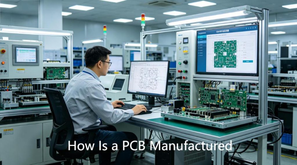
What Is the General Process When a PCB Is Manufactured?
Understanding how is a PCB manufactured helps technical personnel grasp core production workflows, and knowing how is a PCB manufactured also enables designers to optimize files for smoother fabrication.
A complete printed circuit board workflow includes design validation, substrate preparation, circuit patterning, drilling, surface finishing, and final quality inspection.
Each manufacturing stage follows strict industrial standards to guarantee consistent electrical performance and extended service lifespans for finished circuit boards.
What Preparations Are Needed Before PCB Manufacturing Starts?
Complete design documentation and material confirmation are mandatory before formal PCB fabrication begins.
Designers must finalize Gerber files, layer stackups, and fabrication parameters for manufacturing reference.
Fabricators confirm substrate type, layer count, board thickness, and application requirements in advance.
Potential design flaws are identified at this stage to prevent costly rework during mass production.
How Does Substrate Material Selection Affect PCB Manufacturing Quality?
Base substrate materials directly determine a PCB’s heat resistance, dielectric strength, and industrial applicability.
Different substrates are engineered to withstand distinct temperature ranges and signal transmission requirements.
| PCB Substrate Type | Heat Resistance Level | Main Usage Scene | Manufacturing Feature |
| FR-4 | Medium-high temperature resistant | General consumer and industrial electronics | Stable dielectric performance, easy fabrication |
| Aluminum Substrate | High thermal conductivity | LED lighting, power drive modules | Efficient heat dissipation, single-layer focused |
| Ceramic Substrate | Ultra-high temperature resistance | Aerospace, high-frequency precision devices | Superior insulation, complex manufacturing process |
What Are the Core Steps Inside Formal PCB Manufacturing?
Standard single-layer and multilayer PCBs follow a standardized, sequential manufacturing workflow.
Fabrication begins with inner layer etching, followed by lamination for multilayer board bonding.
High-precision mechanical drilling creates vias for electrical interconnection between conductive layers.
Outer patterning, solder mask application, and silkscreen marking are completed in successive stages.
Complete Standard Manufacturing Flow
- Gerber file review and engineering pre-production validation
- Raw substrate cutting and surface chemical cleaning
- Copper foil lamination and inner layer photo-etching
- Multilayer alignment, stacking, and thermal compression
- Precision drilling and electroless copper hole metallization
- Outer circuit imaging and conductive trace modification
- Solder mask coating and thermal curing
- Surface finishing and component identifier silkscreen printing
- Automated electrical testing and final visual inspection
Which Surface Finishing Methods Are Widely Used in PCB Manufacturing?
Surface finishing prevents copper trace oxidation and enhances solderability for component assembly.
Each finishing technique serves different assembly methods and long-term environmental conditions.
Common industry options include HASL, ENIG, immersion silver, and OSP surface treatment.
Manufacturers select suitable finishes based on product lifespan, complexity, and assembly processes.
How to Control Precision Tolerance During PCB Manufacturing?
Strict dimensional tolerance control improves fabrication yield and assembly compatibility.
Advanced industrial machinery regulates trace width, spacing, and hole positional deviation.
Continuous sampling inspections identify and correct mechanical deviations during production.
Design margin optimization effectively lowers manufacturing precision limitations.
What Main Industries Apply Mass-Manufactured PCBs?
Industrially manufactured PCBs support countless electronic sectors with stable, repeatable performance.
Four high-demand industries heavily rely on standardized and custom PCB manufacturing services.
Automotive Electronics Industry
Vehicle control boards and sensor PCBs are mass-produced for automotive electronic systems.
These rigid circuit boards withstand vibration and fluctuating temperatures to ensure driving safety.
Industrial Control & Automation Industry
PLC mainboards and industrial sensor circuits are fabricated for continuous factory operation.
Durable PCBs maintain stable performance within dusty, humid industrial environments.
Medical Electronic Industry
Diagnostic devices and portable medical instruments require high-grade PCB manufacturing.
Strict fabrication standards comply with medical regulations to guarantee detection accuracy.
Communication Equipment Industry
Base station and network communication PCBs demand high-precision low-loss fabrication.
Optimized internal layouts ensure consistent high-speed signal transmission performance.
What Common Defects Occur During PCB Manufacturing?
Most PCB defects originate from inconsistent processing and uncontrolled fabrication parameters.
Residual copper residue frequently causes short circuits after improper etching procedures.
Improper hole cleaning often results in blocked vias and poor electrical conductivity.
Insufficient curing time commonly leads to peeling or brittle solder mask layers.
Low-quality surface finishing negatively impacts component solderability during assembly.
How to Optimize Design to Simplify PCB Manufacturing Process?
Early design optimization minimizes manufacturing complexity and improves production yield rates.
Overly dense routing and irregular hole layouts significantly increase fabrication difficulty.
Unified pad specifications streamline automated assembly and manufacturing workflows.
Limiting complex cutouts and irregular geometries shortens overall production cycles.
We support on-demand customization for all circuit board revisions and provide free DFM reports to eliminate manufacturability risks.
How to Complete Strict Quality Testing After PCB Manufacturing?
All finished PCBs undergo comprehensive testing before shipment to ensure industrial reliability.
Automated electrical testing detects open circuits, short circuits, and conductive failures.
Thermal cycling aging validates structural stability under extreme temperature fluctuations.
Manual visual inspection identifies cosmetic flaws including silkscreen misalignment and surface scratches.
Sampling solderability tests verify soldering performance for downstream assembly procedures.
FAQ – Common Questions About PCB Manufacturing
Q1: What is the normal production cycle for ordinary manufactured PCBs?
A: Standard single and double-layer PCBs take 3–5 working days for completion, while high-precision multilayer boards require extended production timeframes.
Q2: Can special-shaped customized circuit boards be manufactured in batches?
A: Yes. Mature fabrication technology supports non-standard outlines, customized cutouts, and specialized functional PCB mass production.
Q3: Does PCB manufacturing support environmentally friendly halogen-free standards?
A: Modern production lines utilize halogen-free raw materials to comply with international environmental compliance regulations.
Q4: What is the maximum layer count achievable in regular PCB manufacturing?
A: Standard fabrication processes reliably produce 2–16 layer PCBs to satisfy most industrial and consumer electronic requirements.
Q5: Will design modification affect the overall PCB manufacturing progress?
A: Minor early-stage adjustments have negligible impact; large layout revisions mid-production will noticeably delay delivery schedules.
Reliable Custom PCB Manufacturing Service From Thindry
We deliver one-stop PCB manufacturing services covering design optimization, batch fabrication, and industrial quality testing.
Custom production workflows are tailored for different industries to guarantee long-term board stability.
We support on-demand customization for all printed circuit board types and providefree DFM reports to minimize potential production defects.
For PCB prototyping, mass manufacturing, or technical design consultation, contact our experienced engineering team anytime. Reach out to Thindry via official email: sales@pcbtry.com to receive customized PCB manufacturing solutions.


0 Comments