
You can easily identify a PCB ballast through visual inspection, component testing, and circuit layout verification, and this guide simplifies every identification step for beginners and industry practitioners. A PCB ballast refers to an integrated ballast circuit printed on a bare printed circuit board, commonly used for power regulation of lighting and electronic driving equipment. This article covers practical identification methods, key distinguishing features, industry application cases, and common troubleshooting to help users accurately recognize PCB ballasts in various electronic projects.
1. What Is the Fastest Way to Identify a PCB Ballast?
The fastest method to identify a PCB ballast is visual physical inspection combined with basic multimeter testing, which takes less than five minutes without complex professional equipment. This method suits daily inspection, component screening and on-site maintenance scenarios for all technical personnel.
1.1 Visual Inspection (No Tools Required)
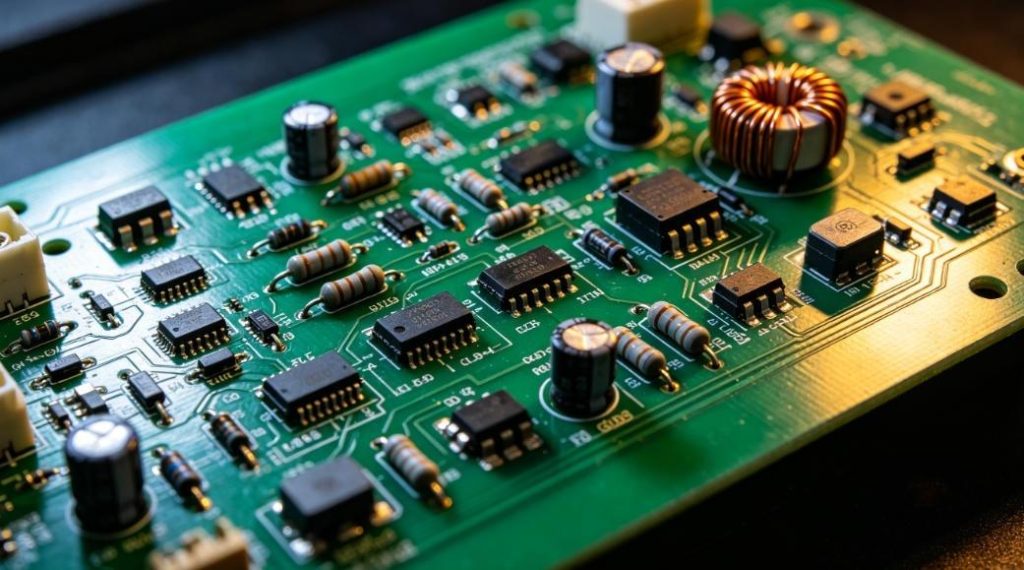
- Circuit Layout: Look for compact high-frequency circuit areas with dedicated lamp connection pads on the PCB.
- Core Components: Check for high-voltage electrolytic capacitors, MOSFET transistors, and pulse transformers, which are standard ballast parts.
- Marking Labels: Qualified PCB ballasts are printed with voltage parameters such as 120V, 220V or 277V on the board surface.
1.2 Multimeter Auxiliary Testing
Set the multimeter to capacitance and diode gears to test key components. Normal PCB ballasts have stable capacitance values and no short-circuit faults in power tubes.
2. What Key Components Does a Standard PCB Ballast Contain?
A qualified PCB ballast consists of six fixed core electronic components, and recognizing these parts is the core basis for accurate identification. Different from ordinary power PCBs, these components are matched for high-frequency voltage conversion to drive lighting loads.
Core Component List for PCB Ballast Identification
| Component Name | Functional Purpose | Visual Identification Feature |
| High-voltage Electrolytic Capacitor | Stabilize rectified DC voltage | Cylindrical shape, marked with 400V/450V voltage rating |
| Pulse Transformer | Boost high-frequency pulse voltage | Small enclosed magnetic ring with copper winding |
| MOSFET Power Transistor | Control high-frequency switching circuit | Flat patch component with three pins |
| Rectifier Bridge | Convert AC to DC current | Square four-pin integrated rectifier module |
| Resistor Bank | Limit current and protect circuit | Black patch resistors with precision resistance codes |
| Drive IC Chip | Adjust frequency and output power | Small SOP-8 packaged integrated chip |
3. How to Differentiate PCB Ballast vs Traditional Inductive Ballast?
Most users confuse PCB ballasts with inductive ballasts; a clear structural and performance comparison can complete rapid differentiation. PCB ballasts adopt fully integrated circuit design, while inductive ballasts rely on bulky copper coils.
PCB Ballast VS Inductive Ballast Comparison Table
| Comparison Dimension | PCB Ballast | Traditional Inductive Ballast |
| Structure Form | Compact printed circuit board integration | Large independent copper coil structure |
| Working Frequency | 20kHz – 60kHz high frequency | 50Hz/60Hz industrial frequency |
| Heat Generation | Low heat, stable long-term operation | Severe heat generation, high energy consumption |
| Application Scenario | Miniature lighting and intelligent equipment | Industrial high-power fluorescent lamps |
| Service Life | 50,000+ hours | 20,000 – 30,000 hours |
4. What Common Industry Applications Use PCB Ballasts?
PCB ballasts are widely applied in four mainstream industries due to their miniaturization and high stability. Each industry has customized PCB ballast designs to solve targeted power drive problems.
4.1 LED/Lighting Industry
This is the most extensive application industry for PCB ballasts. Customized PCB ballast boards are used for LED tube lights and panel lights.
It solves stroboscopic and unstable current problems, improving lighting comfort and service life.
4.2 Industrial Control/Automation Industry
Industrial indicator lights and automated pipeline lighting adopt high-temperature resistant PCB ballasts.
The reinforced PCB structure adapts to harsh industrial environments and avoids circuit failure caused by temperature fluctuation.
4.3 Automotive Electronics Industry
Vehicle interior ambient lights and exterior warning lights use miniaturized PCB ballasts.
It resists vehicle vibration and voltage surge to ensure stable lighting during driving.
4.4 Power/Electronic Power Industry
Low-voltage power distribution indicator equipment applies insulated PCB ballasts.
It realizes safe voltage conversion and prevents short-circuit risks in power distribution systems.
5. What Defective Signs Can Be Observed on a Faulty PCB Ballast?
You can identify damaged PCB ballasts through obvious surface defects, which helps users quickly screen unqualified boards in procurement and maintenance. These visual signs are intuitive and do not require professional testing tools.
- Capacitor Bulging: The top of electrolytic capacitor bulges or leaks electrolyte, indicating aging failure.
- Circuit Board Carbonization: Black burnt marks appear on the PCB copper foil caused by overcurrent burnout.
- Solder Joint Cracking: Welding points of transformer and MOSFET fall off due to long-term vibration.
- Component Deformation: Irregular deformation of chip components caused by high-temperature baking.
6. How to Test PCB Ballast Electrical Performance Accurately?
After completing visual identification, professional electrical testing can verify the working performance of PCB ballast to eliminate hidden internal faults. Three simple testing steps are suitable for technical inspectors and procurement personnel.
6.1 No-load Voltage Test
Connect the PCB ballast to rated power without load, and measure output voltage with a multimeter.
Normal no-load voltage ranges from 300V to 400V; excessive or low voltage indicates circuit abnormality.
6.2 Load Operation Test
Connect matched fluorescent or LED lamps to observe startup status and lighting stability.
Qualified products achieve instant startup without flicker or audible buzzing noise.
6.3 Temperature Rise Detection
Continuously power on the PCB ballast for 30 minutes to detect surface temperature.
The normal temperature shall not exceed 65°C; overheating means unreasonable circuit design.
7. What Mistakes Should Be Avoided When Identifying PCB Ballasts?
Many users make common identification errors leading to misjudgment of PCB ballast types and quality. Summarized industry mistakes can improve identification accuracy for all users.
- Mistake 1: Confusing ordinary power supply PCB with ballast PCB, ignoring high-frequency circuit characteristics.
- Mistake 2: Judging quality only by appearance, ignoring internal solder joint and layer structure.
- Mistake 3: Using mismatched voltage for testing, resulting in component burnout.
- Mistake 4: Neglecting environmental adaptability, ignoring high and low temperature resistance parameters.
8. FAQ: Frequently Asked Questions About PCB Ballast Identification
This FAQ section sorts out high-frequency industry questions about how to identify a PCB ballast, answering core doubts for designers, purchasers and maintenance personnel concisely.
8.1 Can I identify a PCB ballast without a multimeter?
Yes, you can complete basic identification through visual inspection only. Focus on component distribution, printed parameters and board shape to distinguish PCB ballasts from other circuit boards.
8.2 What is the standard size of a regular PCB ballast?
Civil lighting PCB ballasts are usually 50mm×30mm to 120mm×50mm. Industrial high-power models have larger sizes with thicker copper foil for heat dissipation.
8.3 Why does my PCB ballast keep flickering after installation?
Flickering is caused by aging capacitors, damaged drive IC or mismatched load parameters. Replace faulty components or reselect matched PCB ballast products.
8.4 Are PCB ballasts suitable for outdoor high-humidity environments?
Ordinary PCB ballasts cannot be used outdoors. You need customized waterproof and insulated PCB ballasts with conformal coating protection for humid outdoor scenarios.
8.5 How to distinguish genuine and refurbished PCB ballasts?
Genuine products have clear silk screen printing, smooth solder joints and uniform component arrangement. Refurbished boards have worn silk screens and oxidized component pins.
8.6 Do PCB ballasts need customized circuit parameters?
Yes, different industries and equipment require customized voltage, frequency and power parameters. Personalized design ensures stable operation in specific application scenarios.
9. Professional PCB Ballast Manufacturing & Customization Services
This guide covers all practical methods toidentify a PCB ballast, helping users quickly judge product quality and application suitability. Whether you are engaged in circuit design, component procurement or equipment maintenance, standardized identification processes can reduce selection errors and maintenance costs.
Thindry provides professional PCB and PCBA manufacturing services focusing on customized PCB ballast solutions for lighting, automotive, industrial control and power industries. We support on-demand customization and offer free DFM reports for every customized project to optimize circuit structure and avoid production risks.
If you have any PCB ballast production, customization or sample ordering demands, feel free to contact our professional technical team. Send your design requirements to sales@pcbtry.com, and we will provide one-stop electronic circuit manufacturing solutions for you.
0 Comments