
What Is the Simplest Way to Change PCB Board Size in Ultiboard?
You can change PCB board size in Ultiboard quickly using the board outline editing tool without redrawing your entire circuit layout. Mastering how to change PCB board size in Ultiboard helps hardware designers adjust dimensions for enclosures, assembly requirements, and industrial standardization.
Most beginners waste time reimporting files or redrawing borders. Ultiboard provides native editing functions to resize boards while keeping traces, pads, and components untouched.
Why Do Engineers Need to Resize PCBs Inside Ultiboard?
PCB resizing is a frequent modification during prototyping and iteration. Layout adjustments, enclosure limitations, and component rearrangement force designers to alter board dimensions before manufacturing.
- Enclosure fitting: Electronic housing often requires compact or modified board boundaries.
- Prototype iteration: Adjusting sizing to test different assembly layouts.
- Cost optimization: Removing empty PCB space to reduce raw material usage.
- Standard compliance: Matching industry standard PCB form factors for mass production.
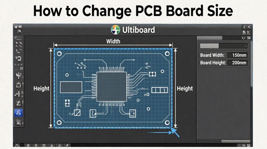
How to Edit Board Outline to Change PCB Board Size in Ultiboard
Step 1: Enable Board Outline Editing Mode
Open your Ultiboard project and locate the outline layer. Double-click the board border to activate boundary modification mode.
Locked borders require you to disable protection under design properties before making any dimensional changes.
Step 2: Modify Border Vertices Manually
Click any vertex of the PCB outline to drag and reshape the board. You can add new anchor points for irregular PCB shapes.
Keep edge spacing consistent to avoid manufacturing errors during PCB fabrication.
Step 3: Input Exact Dimension Values
For precise sizing, open the board property panel and type exact width and height parameters. This method eliminates manual dragging errors.
Always confirm unit settings (mm or inch) to match your manufacturing standard.
Step 4: Recheck Component Clearance
After resizing, run a quick clearance check. Ensure no pads or traces overlap the new board edge.
Remove floating copper and redundant tracks to maintain design integrity.
How to Resize Irregularly Shaped PCBs in Ultiboard
Irregular PCBs with cutouts, notches, and curved edges require vertex editing instead of basic dimension input. Ultiboard supports free-form boundary modification for non-rectangular circuit boards.
Use the polygon drawing tool to redraw custom borders. Delete old outlines after confirming the new board shape.
Complex cutouts must be assigned to the correct mechanical layer for fabrication recognition.
What Common Mistakes to Avoid When Resizing Ultiboard PCBs
Improper resizing often causes broken traces, clearance violations, and unmanufacturable board outlines. Most design errors happen due to unchecked layer settings.
| Common Mistake | Negative Impact | Correct Solution |
| Ignoring mechanical layers | Manufacturers cannot recognize custom borders | Save outlines on Mechanical 1 layer |
| Moving components without clearance check | Edge short circuits and exposed copper | Maintain minimum 0.3mm edge clearance |
| Mixing inch and mm units | Abnormal board dimension output | Unify measurement unit before editing |
| Resizing without DFM inspection | Mass production failure | Run design verification after every resize |
How to Move Components After Changing PCB Board Size
Once you modify board boundaries, scattered components need rearrangement. Ultiboard includes an auto-align tool to optimize component placement rapidly.
Select all surface-mounted parts and use the alignment menu to standardize spacing. Avoid manual random dragging for dense layouts.
Re-route broken tracks and verify impedance continuity for high-speed signal circuits.
Ultiboard vs Other EDA Software: Which Is Better for PCB Resizing?
Each electronic design automation tool has different boundary editing logic. Ultiboard is beginner-friendly for simple dimension modification, while advanced software requires complex layer setup.
| Software | PCB Resize Difficulty | Best Usage Scenario |
| Ultiboard | Easy | Education, simple prototype PCB |
| KiCad | Moderate | Open-source medium-complexity layout |
| Altium Designer | Moderate | High-density commercial PCB |
| Eagle CAD | Hard | Fixed-size industrial circuit boards |
How to Export Correct Gerber Files After Resizing PCB in Ultiboard
Updated board sizes require re-exported Gerber files to avoid mismatched manufacturing data. Old Gerber files will still retain original dimensions.
Enable all production layers including solder mask, silkscreen, and mechanical outline during exporting.
Check file resolution and confirm border coordinates match your modified PCB size parameters.
Real Industrial PCB Cases After Ultiboard Dimension Modification
Consumer Electronics
Wearable smart sensors require ultra-compact PCB layouts. Designerschange PCB board size in Ultiboard to shrink boards for tiny plastic enclosures. This modification reduces overall device weight without sacrificing circuit functions.
Automotive Electronics
Automotive sensor PCBs need fixed irregular shapes to fit vehicle gaps. Engineers adjust Ultiboard outlines to create asymmetric borders that resist vibration and temperature fluctuation inside car modules.
Industrial Control
PLC auxiliary circuit boards often require standardized sizing. Resizing simplifies installation inside industrial cabinets and ensures compatibility with universal mounting brackets.
Medical Electronics
Portable diagnostic devices need slim and safe PCB structures. Precise dimension adjustment avoids sharp edges and meets medical-grade safety requirements for long-term portable usage.
How to Preview Manufacturing Feasibility After PCB Resizing
Any size change may create unmanufacturable parameters such as narrow edge spacing or abnormal cutouts. A design preview helps eliminate hidden risks.
Check minimum trace width, hole spacing, and solder mask coverage after every resize operation.
Professional manufacturability inspection ensures stable mass production yields.
FAQ: Common Questions About Changing PCB Board Size in Ultiboard
Q1: Can I resize a finished PCB layout without deleting components?
A: Yes. Ultiboard supports border modification without removing components. All traces and footprints remain intact as long as you do not overwrite layout layers.
Q2: Why is my Ultiboard PCB outline locked and uneditable?
A: Locked borders are caused by protected mechanical layers. Unlock board outlines in design property settings to enable vertex dragging and dimension editing.
Q3: Does resizing affect Gerber file generation?
A: Yes. You must re-export Gerber files after changing PCB size. Outdated files will produce circuit boards with original unmodified dimensions.
Q4: Can I create curved PCB edges inside Ultiboard?
A: Yes. Add extra anchor vertices and drag points to form smooth curved borders. Save customized shapes on the mechanical layer for fabrication recognition.
Q5: Is Ultiboard suitable for high-density industrial PCB resizing?
A: Ultiboard works best for low-to-medium density boards. For complex high-layer industrial PCBs, export modified files to advanced EDA software for further optimization.
Q6: What is the safest edge clearance after PCB resizing?
A: Maintain a minimum 0.3mm clearance between components and board edges to prevent copper exposure and assembly damage.
Why Choose Thindry for Post-Editing PCB Manufacturing
After you change PCB board size in Ultiboard, reliable fabrication becomes critical for design consistency. Improper manufacturing leads to dimension deviation and assembly failure.
Thindry provides support for customized solutions and free DFM reports for all modified Ultiboard PCB designs. Our engineers inspect borders, clearance, layer alignment, and manufacturability in detail.
Whether you need prototype PCB, mass production, or customized circuit modification services, contact our professional team at sales@pcbtry.com to place your order.
0 Comments