
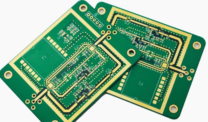
ENIG finish in PCB (Electroless Nickel Immersion Gold) is a widely used two‑layer metallic surface coating for printed circuit boards. This ENIG finish in PCB protects copper pads, improves solderability, and enhances long‑term reliability for high‑performance electronics. If you design or manufacture PCBs for medical, aerospace, or industrial equipment, understanding ENIG is critical to avoiding assembly failures and ensuring stable performance.
What Is ENIG Finish in PCB? – Full Explanation
ENIG finish in PCB is a chemical coating process that deposits a nickel‑phosphorus alloy layer and a thin immersion gold layer onto exposed copper surfaces. It uses no electric current, resulting in uniform thickness across the entire board.
- The nickel layer acts as a diffusion barrier and provides mechanical strength.
- The gold layer prevents oxidation and preserves solderability during storage and handling.
How Does ENIG PCB Surface Finish Work?
ENIG relies on a series of controlled chemical reactions to form a robust protective layer.
- Cleaning and conditioning to remove organic and inorganic contaminants
- Microetching to activate the copper surface
- Catalyst application for nickel deposition
- Electroless nickel plating (Ni‑P alloy)
- Immersion gold displacement reaction
- Final rinsing and drying
What Are the Key Advantages of ENIG Finish?
- Ultra‑flat surface ideal for fine‑pitch components and BGA packages
- Excellent oxidation resistance and long shelf life (12–18 months)
- Compatible with lead‑free soldering and multiple reflow cycles
- Strong electrical conductivity and reliable contact performance
- Suitable for wire bonding and switch contact applications
What Are the Limitations of ENIG in PCBs?
- The process requires tight chemical control to prevent defects.
- Risk of black pad formation if the nickel layer is improperly processed.
- Nickel may slightly degrade signal integrity in ultra‑high‑frequency RF designs.
- More complex than basic surface finishes such as OSP or HASL.
What Are the Standard Thickness Specifications for ENIG?
Standard industrial specifications for ENIG finish in PCB:
- Nickel layer: 3–5 μm
- Gold layer: 0.05–0.1 μm
These values ensure strong solder joints and consistent long‑term performance.
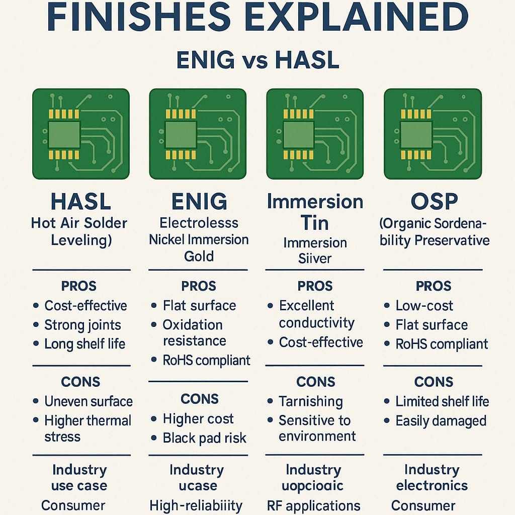
How Does ENIG Compare to HASL, OSP, Immersion Silver, and Tin?
| Feature | ENIG | HASL | OSP | Immersion Silver | Immersion Tin |
|---|---|---|---|---|---|
| Surface Flatness | Excellent | Poor | Excellent | Very Good | Very Good |
| Shelf Life | 12–18 months | 6–12 months | 2–6 months | 6–12 months | 6–12 months |
| Fine‑Pitch / BGA | Best | Not suitable | Good | Good | Good |
| Oxidation Resistance | Excellent | Good | Low | Moderate | Moderate |
| Lead‑Free Compatible | Yes | Yes | Yes | Yes | Yes |
Why Is ENIG Preferred for BGA and Fine‑Pitch PCBs?
ENIG delivers an extremely flat and uniform surface, eliminating unevenness that causes weak or unreliable solder joints in BGAs, QFNs, and components below 0.5 mm pitch. This stability reduces assembly defects and improves production yields in high‑density PCB designs.
What Industries Use ENIG Finish Most Often?
ENIG finish in PCB is widely adopted in these high‑reliability sectors:
- Medical devices (patient monitors, diagnostic imaging, implantable equipment)
- Aerospace and avionics (flight controls, satellite systems, radar modules)
- Industrial automation (PLCs, sensors, motor drives, robotics)
- Automotive electronics (ADAS, infotainment, engine control units)
- High‑end consumer electronics and telecommunications equipment
Real‑World ENIG PCB Examples: Medical, Aerospace, Industrial
Medical Electronics
ENIG is widely used in surgical instruments, diagnostic devices, and portable patient monitors. Its biocompatibility, oxidation resistance, and consistent solderability meet strict medical regulatory and quality requirements.
Aerospace & Avionics
ENIG PCBs are used in radar systems, communication modules, and flight control units. They perform reliably under extreme temperatures, vibration, and humidity for long‑life aerospace applications.
Industrial Equipment
ENIG provides stable performance in factory automation, robotics, and power controllers. It withstands harsh industrial environments including dust, moisture, and wide temperature fluctuations.
How to Avoid Black Pad Issues in ENIG PCBs?
Black pad is a brittle nickel‑gold interfacial defect that weakens solder joints. To prevent it:
- Partner with a reputable PCB manufacturer with stable ENIG process control.
- Maintain proper nickel phosphorus content (6–9 wt%).
- Avoid over‑etching or excessive immersion gold dwell time.
- Perform quality inspections including cross‑section analysis and solderability testing.
FAQ About ENIG Finish in PCB
What does ENIG stand for in PCB?
ENIG stands for Electroless Nickel Immersion Gold, a two‑layer chemical surface finish for printed circuit boards.
Is ENIG finish good for PCB?
Yes, ENIG finish in PCB is an excellent choice for high‑reliability, fine‑pitch, and long‑shelf‑life applications.
How long can ENIG PCBs be stored?
ENIG PCBs can typically be stored for 12–18 months when kept in sealed, dry packaging.
Can ENIG be used for wire bonding?
Yes, with proper nickel thickness control, ENIG supports both aluminum and gold wire bonding.
Is ENIG lead‑free and RoHS compliant?
Yes, ENIG is lead‑free and fully compliant with RoHS and other global environmental standards.
Does ENIG work for high‑frequency PCBs?
ENIG performs well in most high‑frequency designs. The nickel layer may cause minor signal loss in extreme RF or microwave applications.
What is the difference between ENIG and ENEPIG?
ENEPIG includes a palladium layer between nickel and gold, which further reduces black pad risk for ultra‑high‑reliability applications.
Can ENIG PCBs be reworked?
Yes, ENIG PCBs can be reworked using standard SMT rework and repair processes.
How to Order High‑Quality ENIG PCBs?
When ordering ENIG finish in PCB, verify these critical factors:
- Standard thickness: Ni 3–5 μm, Au 0.05–0.1 μm
- Stable process control to eliminate black pad risk
- Compliance with IPC standards
- Material and performance matching your application environment
We provide professional ENIG finish in PCB manufacturing services for medical, aerospace, industrial, and high‑tech electronics. If you need high‑quality ENIG PCBs, please place your order with us. Contact us at: sales@pcbtry.com – Thindry.


0 Comments