
Smart home devices are reshaping how people interact with lighting, security, climate control, and appliances. Behind every smart switch, thermostat, or sensor is a carefully engineered printed circuit board (PCB) that enables connectivity, intelligence, and reliable operation. As smart home products move toward higher integration, wireless connectivity, and 24/7 operation, smart home PCB design and assembly have become critical to product performance, safety, and scalability.
This guide explains what a smart home PCB is, how it is designed, the technologies it uses, and what to consider when manufacturing smart home PCBs at scale.
What Is a Smart Home PCB?
A smart home PCB is the core electronic platform that powers connected home devices. It integrates control, sensing, power management, and wireless communication on a single board or a compact multi-board system.
Compared with traditional consumer electronics PCBs, smart home PCBs typically feature:
- Embedded wireless connectivity
- Low-power or ultra-low-power operation
- Continuous uptime and long service life
- Compliance with global safety and EMC standards
Smart home PCBs act as the “brain” of IoT-enabled home systems, allowing devices to collect data, communicate with networks, and respond intelligently to user commands or automation rules.
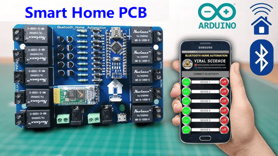
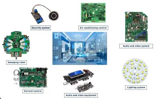
Common Smart Home Devices Using PCBs
Smart home PCBs are widely used across many product categories, including:
- Smart light bulbs, switches, and dimmers
- Smart thermostats and HVAC controllers
- Smart locks, video doorbells, and access control systems
- Motion, door, smoke, and environmental sensors
- Smart plugs, power strips, and energy meters
- Smart appliances such as air purifiers and washing machines
- Voice assistants and smart home hubs
Each application places different demands on PCB size, power consumption, RF performance, and reliability.
Key Components on a Smart Home PCB
A typical smart home PCB includes the following critical components:
- Microcontrollers (MCUs) or SoCs – Execute firmware, process data, and control peripherals
- Wireless modules – Enable communication via Wi-Fi, Bluetooth, Zigbee, Thread, or Matter
- Sensors – Temperature, humidity, motion, light, gas, or proximity sensors
- Power management circuits – AC-DC conversion, DC-DC regulators, battery charging ICs
- Memory devices – Flash or EEPROM for firmware and configuration storage
- Protection components – ESD diodes, fuses, surge suppressors
- Connectors and interfaces – USB, UART, SPI, I²C, test pads
Component selection directly affects product lifespan, certification success, and manufacturing yield.
Smart Home PCB Design Considerations
Designing a smart home PCB requires balancing wireless performance, power efficiency, safety, and manufacturability. Unlike conventional consumer electronics, smart home devices often operate 24/7 and must remain stable over many years. Key design considerations include:
1. Low-Power & Energy Efficiency
Many smart home products are battery-powered or expected to meet ultra-low standby power requirements. Typical targets include:
- Sleep current below 10–20 µA for battery-powered sensors
- Standby power below 0.5 W for AC-powered smart devices
Efficient power architecture, low-Iq regulators, and optimized firmware–hardware interaction are essential.
2. RF Layout and Antenna Design
Wireless performance is highly sensitive to PCB layout. Poor RF design can reduce communication range by 30–50%. Key practices include:
- Controlled-impedance RF traces
- Ground clearance and keep-out zones around antennas
- Proper isolation between RF, power, and digital circuits
3. EMI / EMC Compliance
Smart home PCBs must comply with FCC Part 15, CE EN 55032, and related standards. High-speed clocks, DC-DC converters, and wireless modules increase EMI risk, requiring:
- Solid ground planes
- Short return paths
- Shielding and filtering components
4. Thermal Management
Compact enclosures limit airflow. Even low-power SoCs can generate localized heat. Designers must consider:
- Copper pours and thermal vias
- Component placement to avoid hot spots
- PCB material selection (e.g., Tg and thermal conductivity)
5. Design for Manufacturability (DFM)
Smart home products are often produced in medium-to-high volumes. DFM considerations—such as standard package sizes, optimized panelization, and solder joint reliability—can improve yields by 5–10% and significantly reduce production costs.
Wireless Technologies Used in Smart Home PCBs
Wireless connectivity is the foundation of smart home functionality. Common technologies include:
- Wi-Fi – High bandwidth for cameras, displays, and hubs
- Bluetooth / BLE – Low power, short-range communication
- Zigbee – Mesh networking for lighting and sensors
- Thread – IP-based, low-power mesh protocol
- Matter – Interoperability standard across ecosystems
Smart home PCBs may use PCB antennas, ceramic antennas, or external antennas depending on space and performance requirements.
Reliability & Safety Requirements for Smart Home PCBs
Because many smart home devices operate continuously and connect to household power, reliability and safety are essential:
- Long-term operational stability (24/7 usage)
- Protection against overvoltage, overheating, and short circuits
- Fire-resistant materials and safe power design
- Compliance with standards such as FCC, CE, UL, IEC
- Environmental resistance to humidity and temperature changes
- RoHS and REACH compliance for global markets
High-quality PCB fabrication and assembly play a key role in meeting these requirements.
Common Challenges in Smart Home PCB Projects
Despite mature technologies, smart home PCB development still presents several recurring challenges:
1. Wireless Interference and Signal Instability
Crowded 2.4 GHz environments (Wi-Fi, Bluetooth, Zigbee) can cause packet loss and latency. In real-world deployments, interference can reduce effective data throughput by 40% or more if not properly mitigated.
2. Power Noise Affecting RF and MCU Performance
Switching regulators and digital circuits can introduce noise that degrades RF sensitivity. Insufficient decoupling or poor grounding may lead to intermittent connectivity issues that are difficult to debug.
3. Miniaturization vs. Reliability
As devices become smaller, component density increases. This raises risks such as:
- Solder joint fatigue
- Thermal stress
- Reduced creepage and clearance distances
4. Firmware–Hardware Integration Issues
Smart home devices rely heavily on firmware updates and OTA functionality. Inadequate test points or debugging interfaces on the PCB can slow development and increase failure rates during NPI.
5. Supply Chain and Component Lifecycle Risks
Wireless modules, MCUs, and power ICs are frequently affected by shortages or end-of-life (EOL) notices. Redesigns caused by component obsolescence can add 3–6 months to product timelines if alternatives are not planned early.
Future Trends in Smart Home PCB Technology
Smart home PCB technology continues to evolve rapidly:
- Higher integration using SoCs and system-in-package (SiP) solutions
- Edge AI processing directly on the PCB
- Wider adoption of Matter-enabled devices
- Ultra-low-power and energy-harvesting designs
- HDI PCBs for compact and feature-rich products
- Sustainable materials and greener manufacturing processes
These trends are driving more complex PCB designs with stricter quality requirements.
Why Choose Thindry Circuit for Smart Home PCB & PCBA Services?
Thindry Circuit provides end-to-end smart home PCB and PCBA solutions, supporting customers from concept to mass production.
Our capabilities include:
- One-stop PCB fabrication and assembly for smart home devices
- Expertise in IoT, wireless, and RF PCB assembly
- Prototype, NPI, and volume production support
- Advanced SMT lines for high-mix, low-volume manufacturing
- Strict quality control, functional testing, and traceability
- Manufacturing aligned with global compliance requirements
Ready to accelerate your smart home product development?
Contact Thindry Circuit today for a free DFM review or a custom smart home PCBA quote.


0 Comments