
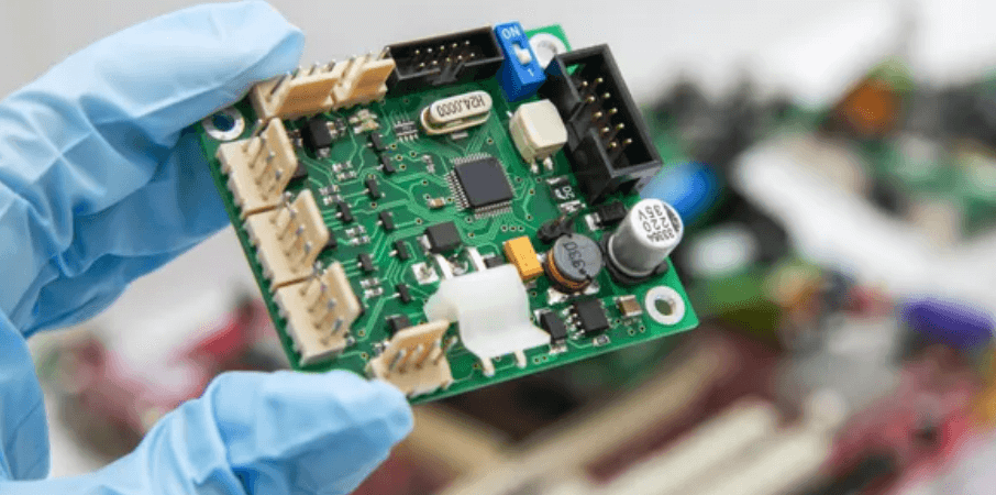
The Internet of Things has moved far beyond consumer gadgets. Today, IoT devices power medical monitoring systems, industrial automation, smart infrastructure, energy management, asset tracking, and mission-critical control networks. At the heart of every reliable IoT device is one foundational element: the IoT PCB.
An IoT PCB is not simply a standard printed circuit board with a wireless chip added. It is a carefully engineered platform that must balance wireless reliability, ultra-low power consumption, compact size, EMI robustness, and long-term manufacturability—often all at once.
This article provides a complete, engineering-driven explanation of what an IoT PCB is, how it differs from conventional PCBs, and how to design and manufacture IoT PCBs that scale from prototype to mass production.
A Complete Guide to IoT PCB Design, Layout, and Manufacturing
What Is an IoT PCB?
An IoT PCB (Internet of Things Printed Circuit Board) is a specialized circuit board designed to enable sensing, data processing, and wireless communication while operating under strict power, size, and environmental constraints.
Unlike traditional PCBs that may prioritize computing performance or power handling, an IoT PCB is optimized around connectivity and efficiency. It must reliably transmit data over wireless networks, often from challenging environments, while consuming minimal energy and maintaining stable performance over long operational lifetimes.
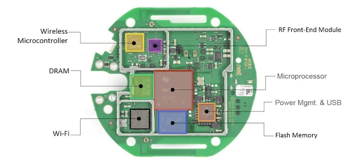
In practice, an IoT PCB integrates:
- A processing unit (MCU or SoC)
- One or more wireless communication interfaces
- Sensors or external I/O
- Power management and battery interfaces
- RF circuitry and antenna structures
The success or failure of an IoT product is frequently determined not by software features, but by PCB-level decisions made early in the design phase.
Essential Components for an IoT PCB
A robust IoT PCB is built from multiple interdependent subsystems. Each must be selected and laid out with system-level awareness.
Processing and Control Core
Most IoT devices rely on low-power microcontrollers or integrated SoCs. These devices handle sensor sampling, data processing, security functions, and protocol stacks.
Key selection criteria include:
- Active and sleep-mode current consumption
- Integrated peripherals (ADC, timers, crypto engines)
- Memory capacity for firmware and OTA updates
- Native support for wireless stacks
Wireless Connectivity Subsystem
Connectivity defines the device’s role within an IoT ecosystem. Common wireless options include:
- Wi-Fi for high data throughput
- Bluetooth Low Energy for short-range, ultra-low-power links
- Zigbee or Thread for mesh networks
- Sub-GHz solutions such as LoRa, NB-IoT, or LTE-M for long-range communication
Wireless selection has direct implications on PCB stack-up, antenna type, component placement, and certification cost.
Sensors and Peripheral Interfaces
IoT PCBs often integrate multiple sensors measuring environmental or physical parameters. These sensors interface via:
- I²C or SPI buses
- Analog signal paths
- UART or GPIO-based triggers
Low-level signal integrity and noise isolation are critical, especially when sensors operate at microvolt or microamp levels.
Power Management Architecture
Power circuitry defines battery life and system stability. A typical IoT PCB includes:
- Primary power source (coin cell, Li-ion, energy harvesting)
- Voltage regulation stages
- Battery charging and protection ICs
- Power sequencing and monitoring
Poor power design is one of the most common causes of early IoT device failure in the field.
Key Considerations in IoT PCB Design
Designing an IoT PCB is an exercise in trade-offs. Several considerations must be evaluated together, not independently.
- Power vs Performance
Higher processing speed and transmit power improve responsiveness but significantly increase energy consumption. Designers must carefully define operating states and duty cycles.
- RF and Digital Coexistence
IoT PCBs often place high-speed digital logic next to sensitive RF circuits. Without careful layout and grounding, these domains interfere with each other.
- Size Constraints
IoT devices are frequently compact or embedded into enclosures that limit PCB area. This increases routing density and EMI risk.
- Lifecycle and Scalability
A design that works for 100 prototypes may fail at 100,000 units due to yield loss, component variation, or assembly limitations.
Typical IoT PCB System Stack-Up
The PCB stack-up is a structural decision that strongly influences RF performance, EMI behavior, and manufacturability.
Common IoT PCB Stack-Up Example (4 Layers)
- Top Layer: RF circuits, MCU, sensors, controlled-impedance traces
- Inner Layer 1: Continuous ground plane
- Inner Layer 2: Power distribution plane
- Bottom Layer: Low-speed routing, debug interfaces, secondary components
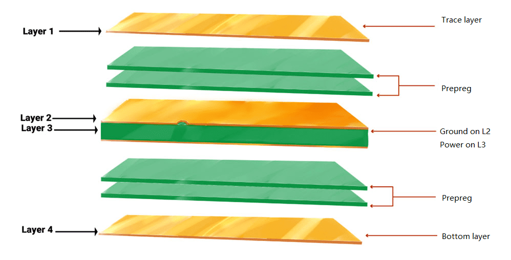
A continuous ground plane is especially critical for antenna reference and EMI suppression. In cost-sensitive designs, 2-layer boards may be used, but often at the expense of RF margin and noise immunity.
Why Does IoT PCB Antenna Layout Cause So Many Wireless Failures?
Antenna design is the single most underestimated aspect of IoT PCB development. Many wireless failures originate not from firmware bugs, but from poor antenna implementation.
Common Antenna Layout Mistakes
- Placing copper pours or signals under the antenna
- Breaking the antenna ground reference plane
- Routing high-speed clocks near the antenna feed
- Ignoring enclosure and battery effects
- Skipping impedance matching or tuning
An antenna that performs well in simulation can fail completely once placed inside a real product enclosure. Successful IoT designs validate antenna performance in final mechanical conditions.
How Do You Choose the Right Wireless Technology for an IoT PCB Design?
Wireless selection should be driven by system requirements, not trends.
Key Evaluation Factors
- Communication range: meters vs kilometers
- Data volume: bytes per day vs continuous streaming
- Power source: coin cell, rechargeable battery, or mains
- Network architecture: point-to-point, star, or mesh
- Deployment region: regulatory and frequency constraints
Selecting the wrong wireless technology early often forces costly PCB redesigns later.
How to Design a Low-Power IoT PCB?
Low-power design is a system-level discipline, not a single component choice.
Effective strategies include:
- Using deep-sleep modes and wake-on-event architectures
- Minimizing leakage paths and pull-ups
- Selecting efficient DC-DC converters at low load
- Power-gating sensors and peripherals
- Optimizing RF transmit intervals and output power
Small PCB-level decisions can translate into months or years of battery life difference.
Why Are EMI and Noise Issues More Critical in IoT PCB Layouts?
IoT PCBs combine sensitive RF circuits, low-level sensors, and noisy digital switching on the same board.
Key challenges:
- Switching regulators injecting noise into RF paths
- Digital clocks coupling into antenna feed lines
- Poor grounding creating common-mode radiation
Robust ground planes, short return paths, proper decoupling, and physical separation between noisy and sensitive circuits are mandatory—not optional.
DFM and DFA Considerations for IoT PCB Assembly
Design for Manufacturability (DFM) and Design for Assembly (DFA) ensure that an IoT PCB can be built consistently at scale.
Critical aspects include:
- Component spacing suitable for automated assembly
- Panelization strategy for small boards
- Controlled impedance and solder mask definitions for RF traces
- Consistent fiducial placement and polarity marking
Neglecting DFM/DFA often results in yield loss or inconsistent RF performance between batches.
Testing and Validation Requirements for IoT PCBA Production
IoT PCBA testing extends beyond basic electrical verification.
Typical validation steps include:
- In-circuit testing (ICT) for assembly integrity
- Functional testing of sensors and MCU
- RF testing for output power, sensitivity, and frequency accuracy
- Power consumption profiling across operating modes
- Environmental and reliability testing when required
Testing strategy should be defined before layout, not after production begins.
FAQ
1. What is an IoT PCB used for?
An IoT PCB is used to host sensors, processing, wireless communication, and power management for connected devices that collect and transmit data.
2. How is an IoT PCB different from a regular PCB?
An IoT PCB emphasizes RF performance, low power consumption, and long-term reliability, whereas regular PCBs may focus mainly on logic or power delivery.
3. Which wireless option is best for my IoT device?
The best option depends on range, power budget, data rate, and network requirements. There is no universal choice.
4. What are the most common mistakes in IoT antenna layout?
Insufficient keep-out zones, broken ground planes, nearby noise sources, and enclosure interference are the most common issues.
5. How do I estimate battery life from PCB design decisions?
Battery life can be estimated by profiling current consumption in each operating mode and summing energy usage over a typical duty cycle.
6. Do I need special testing for IoT PCBA production?
Yes. RF performance, power consumption, and functional validation are essential in addition to standard assembly tests.
7. Should I use a wireless module or a discrete RF design?
Modules reduce risk and certification effort, while discrete RF designs offer cost and size advantages at higher engineering complexity.
8. What files should I send for an IoT PCB/PCBA quote?
Typically Gerber files, drill files, BOM, pick-and-place data, stack-up details, and any specific testing or certification requirements.


0 Comments