
Unlike traditional PCB, which prioritize durability and cost, Clear PCB emphasize visual appeal and aesthetics while ensuring electrical performance. Their high transparency, thinness, flexibility, excellent conductivity, impact resistance, high temperature resistance, and environmental friendliness make them suitable not only for conventional electronic functional carriers but also for various electronic devices requiring optical transparency, structural visualization, or a futuristic appearance.
These advantages have led to the widespread application of Clear PCB in display structural design, visual electronic products, wearable devices, automotive instrument clusters, optical devices, and innovative consumer electronics, making them a crucial material driving differentiated design in next-generation electronic products.
What is a Clear PCB?
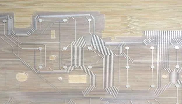
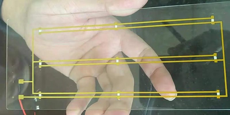
A Clear PCB board is a printed circuit board made with a clear substrate instead of traditional opaque materials (such as FR-4). It breaks through the limitations of the common yellow, black, and white colors of traditional FPC, achieving both circuitry support and visual transparency through a novel material system. These circuit boards are typically made of high-transmittance, high-temperature-resistant PET, glass, or other special clear polymers, with a clear substrate, conductive layer, and insulating layer forming a complete structure.
Material behind clear PCB board
The core advantage of clear PCB lies in their unique substrate structure. Unlike traditional opaque PCB that rely on glass fiber or epoxy resin (such as FR-4), clear PCB use light-transmitting materials, allowing the circuit layers to be both functional and visually appealing. Common clear PCB materials include:
- 1. Glass Substrate:
Glass, with its excellent optical transparency and thermal stability, is the preferred material for high-performance clear PCB. It can withstand high temperatures and harsh working environments, making it ideal for demanding applications such as precision optical systems and display modules. However, glass is also somewhat brittle, requiring extra care during manufacturing and end-use.
- 2. Polymer Films:
Polymer materials used in flexible clear PCB typically include PET or PI. These materials are lightweight and flexible, allowing for bending, rolling, or curved mounting, making them ideal for foldable screen devices, wearable devices, and flexible displays. However, their heat resistance is generally lower than that of glass, making them unsuitable for ultra-high temperature environments.
- 3. Transparent Conductive Materials:
The conductive layer of transparent circuits typically uses materials such as ITO (indium tin oxide) and silver nanowires (Ag NWs) instead of traditional copper foil. These materials provide reliable conductivity while maintaining high light transmittance, forming an important technological foundation for transparent touchscreens and transparent sensors. However, their cost is usually higher than that of traditional metallic conductors.
Techniques for designing PCB using clear boards
When utilizing clear PCB for innovative designs, proper material selection and structural planning are crucial. The following suggestions will help engineers fully leverage the visual and functional advantages of clear circuit boards while ensuring electrical performance:
- 1. Choose a suitable substrate
Select a clear substrate such as glass or polymer film based on project requirements. Glass substrates offer high rigidity and heat resistance, making them suitable for high-temperature environments; polymer films are thin and flexible, making them more suitable for foldable or curved devices. When selecting materials, consider ambient temperature, mechanical stress, and transparency requirements.
- 2. Enhance overall transparency
Minimize the use of opaque components and avoid coatings or screen printing that affect light transmission. Prioritize transparent solder mask layers and transparent adhesives to maximize visual transparency, making internal circuitry an integral part of the design.
- 3. Strengthen signal integrity design
The dielectric constant of transparent substrates differs from traditional FR-4, necessitating impedance control, transmission line simulation, and high-speed signal testing. Ensure critical traces achieve stable, controlled impedance to prevent signal attenuation or distortion due to dielectric differences.
- 4. Partner with Professional Manufacturers
Clear PCB have higher manufacturing barriers, requiring specialized equipment and experience in areas such as material handling, circuit etching, and mounting precision. Choosing a mature manufacturing service provider can effectively reduce processing difficulty and improve yield.
- 5. Emphasize Structural and Aesthetic Design
One of the key values of clear PCB is their visual appeal. Properly planning component layout and circuit routing creates a simple, orderly, and technologically advanced visual effect on the transparent substrate, thereby enhancing product recognition and overall aesthetics.
How are clear PCB manufactured?
The manufacturing process of clear PCB requires balancing optical transparency with electrical performance and structural reliability, making the overall process more rigorous and precise than that of traditional PCB. While the core principles still include etching, patterning, and layering, the details of the process are adjusted due to differences in material properties. The key processes in clear PCB manufacturing are as follows:
- 1. Substrate Preparation
First, the selected clear substrate (such as glass or clear polymer) undergoes thorough cleaning and pretreatment to ensure a smooth and flawless surface. Any minute defects can affect circuit adhesion, optical performance, and ultimately electrical performance; therefore, substrate preparation is fundamental to the entire process.
- 2. Conductive Layer Deposition
A layer of transparent conductive material, such as indium tin oxide (ITO) or silver nanowire coating, is uniformly deposited on the substrate. This layer will serve as the circuit signal conduction path and requires a precise balance between transparency and conductivity.
- 3. Circuit Patterning
Using high-precision processes such as photolithography and laser etching, the conductive layer is patterned into the desired circuit lines. Because some transparent substrates, such as glass, are brittle, the patterning process must strictly control energy and pressure to avoid micro-cracks or damage to the substrate.
- 4. Electronic Component Mounting
Surface mount technology (SMT) is typically used to mount electronic components on clear PCB. For rigid glass substrates, component positioning accuracy is particularly critical. The mounting process must ensure sufficient stability to prevent component misalignment due to thermal or mechanical stress.
- 5. Performance and Optical Testing
The finished circuit board must undergo comprehensive electrical, mechanical, and optical testing, including signal integrity, circuit accuracy, light transmittance, and visual clarity. For high-speed signal applications, impedance control of clear PCB is especially important, typically maintaining the transmission impedance within the range of 50–100 ohms.
The main advantages of clear PCB
Clear PCB not only boast a unique visual appeal, but their performance and application value are equally outstanding. Here are their core advantages:
High Optical Clarity
Clear PCB offer up to 85% light transmittance, providing excellent visual performance in devices with high optical performance requirements and ensuring minimal light loss during transmission.
Excellent Thermal Stability
Some transparent substrates can withstand temperatures of 200°C or even higher, making them ideal for applications with harsh operating environments and significant temperature fluctuations, such as high-brightness display modules, industrial instruments, and outdoor equipment.
SMT Compatibility
Clear PCB fully support standard SMT (Surface Mount Technology) assembly processes. Even on rigid substrates like glass, stable component mounting and soldering are possible, providing a reliable manufacturing foundation for mass production.
High Cost-Effectiveness
Compared to common market prices, the overall cost of Clear PCB can be reduced by 30% to 50%, achieving a more competitive cost advantage without sacrificing quality and performance.
Why choose a clear PCB?
The value of clear PCB lies not only in their aesthetics but also in their ability to meet the comprehensive requirements of modern electronic products for performance, aesthetics, and structural innovation:
- 1. Enhanced Visual Appeal
Clear PCB possess a unique, transparent structure, making them ideal for showcasing internal circuit designs. They are commonly used in consumer electronics, display devices, and new product concept devices where high aesthetics and a technological focus are emphasized.
- 2. Improved Optical Efficiency
In applications such as displays, sensors, and optical modules, clear circuit boards effectively reduce light loss and improve overall optical performance, making them particularly suitable for components with extremely high light utilization requirements.
- 3. Greater Design Freedom
Flexible clear PCB using transparent polymer films can achieve bending, curved surface bonding, and even foldable structures, allowing for greater design freedom and bringing more possibilities for thinner, smaller, and innovatively shaped electronic products.
- 4. Better Thermal Stability
Glass-based clear PCB exhibit particularly excellent high-temperature resistance, with a high-temperature stability of 200°C to 300°C. They are better able to withstand high-temperature environments than traditional FR-4 boards, making them an ideal choice for applications such as laser equipment and high-brightness LED modules.
Challenges of clear PCB
While clear PCB have garnered significant attention in consumer electronics, display technologies, and innovative devices due to their unique visual appeal and superior optical performance, several significant challenges remain in engineering applications and mass production. The following are key considerations for design engineers and manufacturing teams when developing clear PCB:
- 1. Material Fragility
Glass substrates offer excellent thermal stability and optical properties, but their lower mechanical strength makes them prone to breakage under external force or bending. This brittleness limits their use in applications requiring high reliability or resistance to significant mechanical impacts, and necessitates more stringent protective measures during processing, transportation, and assembly.
- 2. Significantly Higher Costs than Clear PCB
Key materials required for clear PCB—such as the ITO (Indium Tin Oxide) clear conductive layer, high-purity glass, or specialty transparent polymers—are more expensive than traditional FR-4 or copper foil materials. Depending on design complexity and material specifications, production costs are typically 20%–30% higher than traditional PCB, with cost pressures becoming even more pronounced in large-scale production.
- 3. High Manufacturing Complexity
The manufacturing of clear PCB cannot completely follow standard PCB processes. Steps such as glass substrate processing, transparent conductive layer deposition, and laser micro-patterning require specialized equipment and more precise process control. This not only increases processing difficulty but also leads to longer production cycles and higher skill requirements for operators.
- 4. Excessively High Conductivity
The resistivity of transparent conductive materials (such as ITO) is significantly higher than that of copper. This means that clear circuits may experience greater energy loss and heat generation in high-current or high-power applications, limiting their use in high-power circuits. Furthermore, the long-term stability and weather resistance of some transparent conductive materials still require further verification.
Common applications of clear PCB
Clear PCB, with their high light transmittance, lightweight structure, and unique visual effects, are increasingly becoming a key component in many innovative electronic products. From wearable devices to display technologies, they not only boast stunning appearances but also offer performance and functionality advantages unmatched by traditional circuit boards.
- 1. Display Technology
Transparency is a core requirement for display applications. clear PCB, achieving up to 85% light transmittance, are widely used in:
LED displays
Transparent screens
Touch panels
AR/VR augmented reality devices
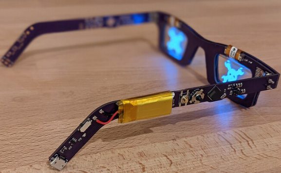
For example, in AR glasses, clear PCB maintain clarity in the user’s field of vision while housing necessary drive circuitry and sensor modules, achieving a balance between aesthetics, lightweight design, and functionality.
- 2. Optical Components
Clear PCB reduce occlusion and light scattering in the optical path, improving the efficiency of optical systems. This is particularly evident in the following devices:
Image sensors
Laser rangefinders
Industrial vision inspection equipment
These applications typically have stringent requirements for high-speed signals. The unique dielectric properties of transparent materials reduce noise interference while maintaining signal integrity.
- 3. Consumer Electronics
Transparent electronics are becoming a design trend in next-generation consumer technology. Clear PCB make internal structures visible, enabling more futuristic designs and are widely used in:
“Visualized” smartphones
Smartwatches
Smartwear accessories
Innovative electronic toys
Transparent designs not only increase product recognition but also give brands a unique technological aesthetic.
- 4. Medical Equipment
In the medical field, clear PCB improve the accuracy of imaging and diagnostic equipment due to their optical advantages. Suitable for:
Medical imaging systems
Surgical navigation instruments
Diagnostic sensing equipment
Transparent substrates allow medical personnel to visually observe optical paths and device positions, making system debugging and maintenance easier.
Industry development of clear PCB
As market demand for thinner, lighter, and more visually striking electronic products continues to rise, clear PCB are gradually moving from a conceptual material to mainstream applications. Advances in materials science, microfabrication processes, and transparent conductive technologies have significantly improved the durability, conductivity, and manufacturing consistency of clear printed circuit boards.
Currently, more and more industries are adopting clear PCB: wearable devices seek lighter and thinner structures; smart home products pursue designs that blend seamlessly with their environment; and the automotive industry is increasingly incorporating transparent display panels to enhance the technological feel of the cockpit. These trends are collectively driving clear PCB from “innovative attempts” to “practical components.” Today’s clear PCB can reliably support high-speed signal transmission, sufficient to meet the needs of future high-performance electronic devices.
At Thindry, we focus on turning clear PCB from concept to reality. Whether customers are designing display PCB or developing unique projects using transparent electronic components, we provide one-stop support from solution consultation and material selection to precision manufacturing and final testing. Our engineering team has in-depth knowledge of the processing characteristics of glass and polymer substrates, ensuring accurate and reliable conductive layer deposition and consistent product performance.
Clear PCB are redefining the look and structure of electronic products, and this is just the beginning. By partnering with Thindry, you will gain access to the full range of technological capabilities to explore the era of transparent electronics, helping you create innovative products that are futuristic and competitively differentiated.


0 Comments