
In modern electronics manufacturing and testing, especially in the semiconductor industry, the load board is a crucial yet often overlooked component. It acts as a “bridge” and “extended stage” between the chip tester and the chip under test (DUT), playing a key role in ensuring chip performance, quality, and reliability.
This article will delve into the definition, complex design considerations, core functions, and wide range of applications of load boards (PCBs).
What is a Load Board PCB? — Definition and Core Concepts
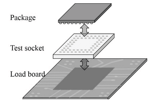
A load board is essentially a highly specialized printed circuit board.
We can understand it as a customized, precision “test adapter.” Its primary mission is to: accurately, non-destructively, and reliably transmit the test resources (such as power, signals, clock, etc.) of automated test equipment to the DUT, and to transmit the DUT’s response signals back to the test equipment for analysis.
Core Components:
PCB Substrate: This is the physical carrier of the load board, typically made of high-performance materials.
DUT Socket: A precision interface used to secure and connect the device under test (DUT). Types include spring-loaded pins and landing pads, requiring a perfect fit to the chip package.
Coaxial Connector/Cable: Used to connect the load board to the ATE (Automatic Test Equipment) system, transmitting high-speed digital, RF, or precision analog signals.
Passive Components: Includes precision resistors, capacitors, and inductors for signal conditioning, decoupling, termination matching, and filtering.
Active Components: In some complex designs, may include buffers, drivers, or clock generators to enhance signal integrity or provide specific test conditions.
Power Distribution Network: A low-noise, low-impedance power supply network that ensures clean, stable voltage and current for the DUT.
In short, without a load board, expensive and powerful automated test equipment cannot directly communicate with tiny, pin-dense modern chips. The load board is this indispensable “translator” and “connector.”
Load Board PCB Functions
The PCB is crucial when using an ATE system to detect design and manufacturing defects in semiconductor devices. It has several unique functions.
ATE to DUT Interface:
It acts as the physical and electrical interface between the Device Under Test (DUT) and the large Automated Test Equipment (ATE) system. This allows the tester to communicate with individual chips and perform electrical checks.
Roading Test Signals:
The circuit board contains complex wiring for transmitting or “loading” test signals from the ATE to the DUT. These components must perform this task efficiently without damaging the delicate integrated circuit (IC) pins.
Power Delivery:
It also powers the DUT, energizing the circuitry for testing. Its components ensure stable and safe voltage. In particular, the Power Distribution Network (PDN) includes decoupling capacitors to ensure stability.
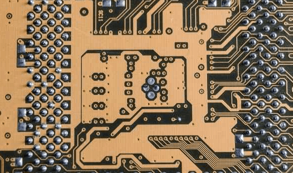
Main Load Board PCB Assembly
This PCB board consists of various components, including pins and sockets, connectors, and heat sinks. It also contains multiple layers for power circuitry, grounding, and signal transmission.
DUT Pins and Sockets:
The sockets hold the integrated circuits in place during testing, ensuring their mechanical stability throughout the testing process. The design of slots varies depending on the integrated circuit package type (e.g., BGA, QFP). They are typically located on the top of the circuit board.
Pin is the electrical contact point between the printed circuit board (PCB) and the integrated circuit (IC). Similar to sockets, they are physically and electrically matched to a specific IC. Furthermore, they must conduct electricity efficiently and allow for reuse.
ATE Tester Connectors:
Connectors transmit power, signals, and data from the tester to the load PCB. In other words, they enable the ATE tester to communicate with the device under test.
Their design and layout must enhance ease of use. They are typically located on the bottom of the circuit board for direct connection to the ATE test head. Given the sophistication of modern integrated circuits, these connectors are also of high-speed type.
Thermal Components:
These are heat dissipation components. They help dissipate heat from the circuit board, preventing it from overheating during use. These components can come in different types depending on the required performance.
Examples include vias, pads, and copper foil. Others include embedded components, such as coins or externally mounted heat sinks. This depends on the type of load board and its intended use.
Power, Ground, and Signal Layers:
This PCB uses separate power, signal, and ground layers. This separation design prevents noise and interference, thus improving PCB reliability, especially in high-frequency and similar applications.
Ground layers are crucial in PCB stack-up structures. They ensure data and signals are not attenuated and require strategic placement to provide shielding.
Load Board Design Considerations – A Combination of Precision and Art
Designing a load board is far more complex than ordinary PCB design; it’s an interdisciplinary challenge involving electrical engineering, RF engineering, and mechanical engineering. The design goal is to achieve test signal integrity while closely mimicking the chip’s actual operating environment.
Key Design Challenges and Considerations:
Signal Integrity:
Impedance Control: High-speed signal traces must undergo strict impedance control (typically 50 ohms or 100 ohms differential) to prevent signal reflection and distortion.
Crosstalk Control: Avoid mutual interference between adjacent signal lines through proper layout, spacing, and ground plane isolation.
Loss Control: For high-frequency signals, PCB materials with low loss factors should be selected, and the skin effect should be considered.
Power Integrity:
Low Impedance Power Network: Utilize complete power and ground planes in a multilayer board and deploy numerous decoupling capacitors to construct a low-impedance power supply network and suppress power supply noise.
Voltage Stability: Ensure that voltage ripple and drop at the power supply pins remain within a minimal range under the dynamically changing current demands of the device under test (DUT).
Thermal Management:
When testing high-power chips, both the load board itself and the DUT generate significant heat. The design must consider heat dissipation holes, heat sinks, or even forced air/water cooling solutions to prevent overheating from affecting test results or damaging the device.
Mechanical Structure and Interface:
Socket Selection: Precision sockets must be selected that match the chip package type, pin pitch, and test life.
Rigidity and Durability: The load board needs to withstand frequent insertions and removals from the test equipment and long-term use; its mechanical structure must be robust and stable.
Interface Alignment: The connection interface with the test equipment must be precisely aligned to ensure reliable and repeatable connections.
Material Selection:
Standard FR-4 material is generally insufficient for high-frequency testing requirements. High-frequency load boards often use high-performance materials with low loss and stable dielectric constants, such as Rogers and Taconic, or are laminated with FR-4.
Core Functions of the Load Board – More Than Just “Connection”
The load board’s function goes beyond simple electrical connection; it plays multiple roles:
Signal Transmission and Routing: The most basic function, accurately routing thousands of test channels from the ATE to specific pins of the chip under test.
Signal Conditioning and Optimization:
Termination Matching: Adding matching resistors at the ends of transmission lines to eliminate signal reflections.
Filtering: Filtering out high-frequency noise on power and signal lines.
Attenuation/Amplification: Adjusting signal levels to meet the input/output requirements of the device under test.
Power Supply and Monitoring: Providing multiple, stable, and clean power supplies to the device under test, and potentially integrating sensors to monitor voltage and current.
Clock Distribution and Synchronization: Provides high-precision, low-jitter clock signals for the device under test (DUT) and ensures clock synchronization in multi-channel systems.
Test Environment Creation: Simulates parts of the chip’s operating environment in real-world applications using on-board components, such as providing simulated physical signal interfaces for sensor chips.
Purpose and Application Scenarios of Load Boards – Ubiquitous Testing Keys
Load boards are used throughout the entire chip lifecycle, from R&D to mass production and failure analysis.
Wafer Testing:
While the chip is still packaged on the wafer, probe cards (a special type of load board) are used to contact the chip pads on the wafer for preliminary electrical testing to screen out faulty dies.
Final Testing:
This is the most typical application scenario for load boards. After the chip is packaged, it is connected to the sockets on the load board for comprehensive functional and parameter testing. Test content includes:
Functional Testing: Verifies the correctness of the chip’s logic functions.
Performance Testing: Tests key parameters of the chip such as speed, power consumption, and frequency.
Reliability Testing: Testing under harsh conditions such as high temperature, low temperature, and high voltage to evaluate chip lifespan and stability.
System-Level Testing:
Testing chips in environments closer to the final product. For example, mounting a processor chip onto a test board simulating a motherboard environment using a load board and running real software or test programs.
Aging Testing:
Persistently powering on chips at high temperature and high voltage to accelerate the aging process and screen out chips with a high risk of early failure (“infant mortality”). Load boards used for this purpose require extremely high reliability and strong heat dissipation capabilities.
Research and Verification:
After tape-out, chip design companies use load boards to conduct in-depth testing and debugging of engineering samples to verify whether the design meets expectations and to provide a basis for the development of mass production test programs.
Conclusion
Load boards (PCBs) are the cornerstone of the modern electronics industry, especially in the field of semiconductor testing. They are far more than simple circuit boards; they are complex systems integrating cutting-edge design, precision manufacturing, and profound engineering understanding. Its performance directly determines the coverage, accuracy, and efficiency of the test, ultimately affecting the quality and cost of the chips shipped from the factory.


0 Comments