
In the field of electronic engineering, Gerber files are a commonly used and standard document type in electronic manufacturing. They help PCB manufacturers produce the circuit boards you design. You can think of them as the standard language for PCB board production, just like code files are for software development. But what if you need to reverse the process and generate PCB files from Gerber files?
In practice, this can happen for various reasons. In such cases, understanding how to convert Gerber files to PCB files is crucial. This is an essential skill in PCB manufacturing, whether you’ve lost your original design, are working with old files, or need to edit an existing project. This guide will introduce you to Gerber and PCB files and guide you step-by-step through the conversion process. After reading this guide, you will be able to perform the conversion with confidence.
What is a Gerber File?
Simply put, a Gerber file is a “digital blueprint” or “standard language” for a circuit board (PCB). It tells PCB manufacturers how to accurately manufacture the circuit board you design.
I. Core Definition and Metaphor
Official Name: Gerber Format, currently the standard is RS-274X (i.e., Extended Gerber).
Core Function: It is a vector format file used to describe the physical structure of each layer of a PCB. It is not an editable design file, but rather the final output file for manufacturing.
A good analogy:
A PCB file (such as Altium Designer’s .PcbDoc or KiCad’s .kicad_pcb) is like a recipe for a dish, containing the ingredients (components), steps (routing logic), and cooking techniques (design rules).
A Gerber file is like a precise, step-by-step breakdown diagram given to the chef (PCB manufacturer). For example, one diagram shows the final plating of the dish (circuit layers), another shows the location for the sauce (solder mask), and another shows the location for the garnish (silicone layer). The chef doesn’t need to know the cooking logic; he only needs to strictly follow these diagrams to make the dish.
II. Key Characteristics of Gerber Files
Storing 2D Vector Data:
It does not store 3D models, schematic connections, or component attributes. It only contains basic geometry: lines, pads, filled areas, and text.
It tells the machine, “Draw a circular copper pad with a diameter of Z at coordinates (X, Y).”
Layered Structure:
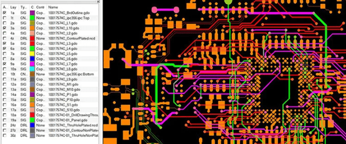
A PCB is made up of multiple layers of materials, and a Gerber file is “one file per layer.”
A complete Gerber file set typically includes:
Top/Bottom Line Layers (GTL, GBL): Defines signal traces and copper foil areas.
Top/Bottom Solder Mask Layers (GTS, GBS): Defines areas where copper needs to be exposed for soldering (usually green paint).
Top/Bottom Silkscreen Layers (GTO, GBO): Defines component borders, identifiers, and text descriptions (usually white ink).
Solder Paste Layers (GTP, GBP): Used for SMT placement, defining the locations where solder paste needs to be applied. Mechanical/Frame Layer (GMx): Defines the physical shape and dimensions of the PCB.
Drill Diagram/Data (DRILL, TXT): A separate drill file that tells the machine where to drill holes and their dimensions.
Computer-readable, human-readable:
You can open a Gerber file with a text editor, but what you’ll see is a series of instruction codes (as shown in the image below), which is very unintuitive to the human eye.
To view Gerber files, you must use specialized “Gerber viewer” software (such as the free Gerbv, GC-Prevue, or the professional CAM350). This software renders the code into a visual graphic.
III. Why is the Gerber format so important?
Industry Standard: It is the universal language of PCB manufacturing. Regardless of the EDA software you use (Altium, KiCad, Eagle, etc.), the final output will be a Gerber file, ensuring that any manufacturer can understand and produce your board.
Intellectual Property Protection: When you give Gerber files to manufacturers, they receive “drawings,” not your original design source files. This protects your core design logic and component libraries to some extent.
Manufacturing Precision: It describes every detail in a precise vector format, ensuring high precision and consistency in production.
What is a PCB File?
A PCB file is an editable file, typically created using PCB design software such as Eagle, KiCad, and Altium. These software programs are widely used, and of course, other software also supports PCB design. PCB files contain design rules, netlists, schematic links (unlike Gerber files), and layout information. Understanding how to convert Gerber files to PCB files is crucial, as this is one of the reasons why converting Gerber files to PCB files is not easy: Gerber files only contain the final physical result, not the design intent.
Why Convert Gerber Files to PCB Files?
You may need to perform this conversion in several situations:
Losing the Original File: Having only the PCB file is risky because if you lose the original Gerber file, you have no backup.
Legacy Projects: Your task is to replace or repair an old circuit board that only has Gerber data.
Reverse Engineering: You’re eager to learn or replicate a design.
Design Improvement: PCB files make it easier to make changes when needed, such as adjusting the board layout to allow for manufacturing in terms of yield, cost, or performance.
In any case, understanding how to convert Gerber files to PCB files can save time, money, and avoid design duplication.
Step-by-Step Guide: How to Convert Gerber Files to PCB Files
- Choosing the Right Software
Many EDA (Electronic Design Automation) systems can import Gerber files and create PCB designs. Commonly used EDA systems include:
Altium Designer, KiCAD, OrCAD/Allegro, Gerber Import (Online), EasyEDA.
- Importing Gerber Files
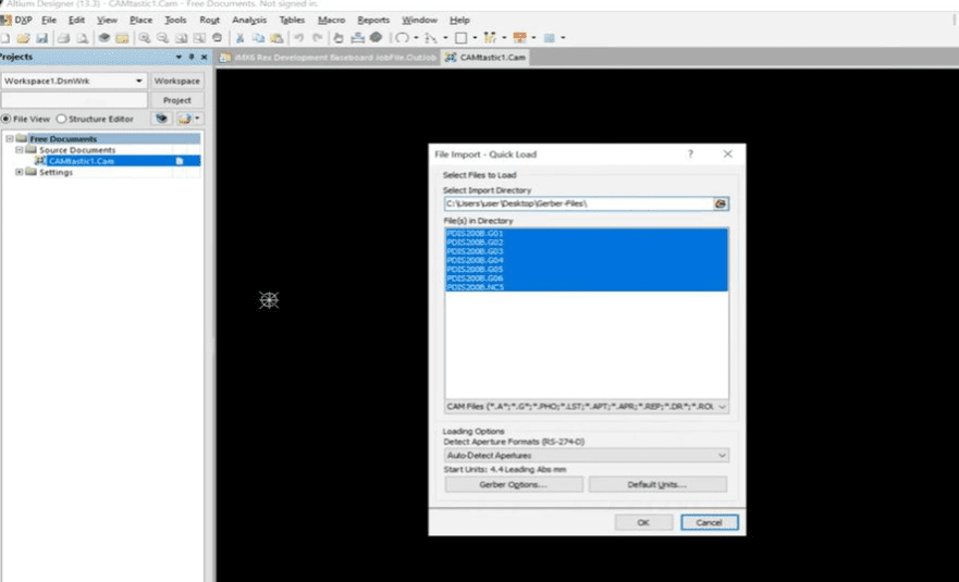
Use the import function to load all the Gerber layers mentioned below.
Top Copper
Bottom Copper
Solder Mask
Silk Screen Printing
Drill File (Excellon)
Ensure the mapping between layers is correct; otherwise, the board will appear misaligned.
- Rebuild Board Layout
The software will display the board outline, pads, and traces after importing. However, you need to define the board dimensions yourself, align the drill holes with the pads, and verify trace connectivity. - Rebuild Netlist
Since Gerber files do not store the netlist, many tools apply algorithms to identify connections. Alternatively, you may need to manually draw the netlist. - Recreate Component Library
The footprints are legible, but symbol and schematic associations are lost. Repair each footprint using the correct parts from the library. - Verify Design
Check for short circuits or open circuits. Verify pad positions and alignment. Verify spacing and trace widths. - Save as PCB Project File
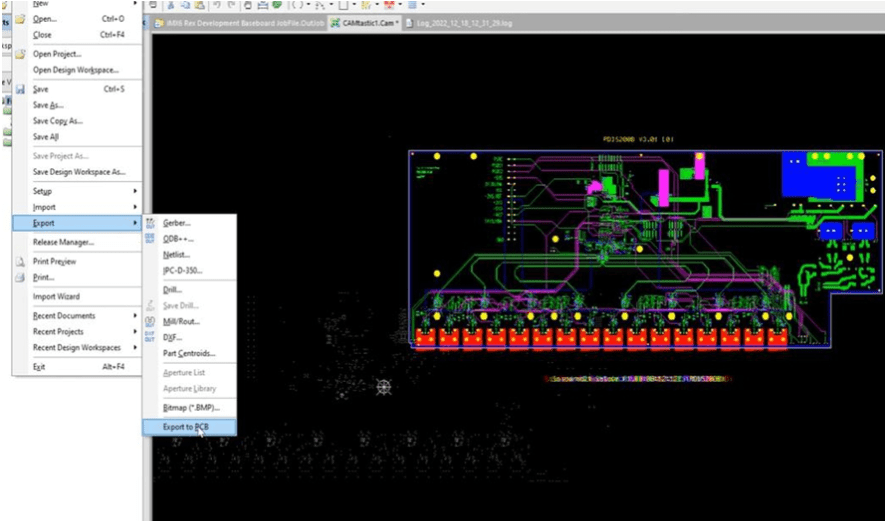
Finally, export the reconstructed board as a native PCB file format (e.g., .pcbdoc in Altium, .kicad_pcb in KiCAD).
Conclusion
Converting Gerber files to PCB files is not easy, but it is achievable with the right tools, knowledge, and processes. Understanding how to convert Gerber files to PCB files ensures a complete, editable, and easily modifiable and reusable layout, even if the original design intent cannot be 100% reproduced.
In modern high-speed design cycles, the ability to convert Gerber files to PCB files can bridge the gap between manufacturing specifications and editable projects, giving engineers greater flexibility, especially when the original files are lost or outdated.
Frequently Asked Questions
Question 1: Can Gerber files be converted to schematics?
Answer: No. Gerber files are not logic circuit files, but only physical layout files. You need to redraw the schematic.
Question 2: What is the most commonly used software for converting Gerber files to PCB files?
The most commonly used software is Altium and KiCAD. EasyEDA is also very easy to use because it’s free and available online.
Question 3: How accurate is the conversion?
Accuracy depends on the completeness of the Gerber kit. Missing drill layers or masking layers will reduce reliability.
Q4. Will manufacturers convert Gerber files to PCB files?
A: No. They do not create PCB files. To obtain PCB files, you must convert them yourself or hire a designer.


0 Comments