
Introduction
PCB wave soldering is an automated soldering process fundamental to electronics manufacturing, particularly for assembling through-hole components onto printed circuit boards. This technology involves passing a PCB over a controlled wave of molten solder, which creates reliable electrical and mechanical connections between component leads and board pads in a high-volume production environment. Since its development in the 1950s, wave soldering has become a cornerstone of electronic manufacturing, enabling efficient mass production of everything from consumer electronics to automotive systems and industrial controls. The process’s ability to simultaneously solder hundreds of components with consistent quality makes it indispensable for cost-effective PCB assembly .
The importance of wave soldering in modern electronics manufacturing cannot be overstated. Despite the growing prevalence of surface-mount technology, wave soldering remains essential for applications requiring the mechanical strength and reliability of through-hole connections. Industry data indicates that properly optimized wave soldering processes can achieve defect rates below 1%, significantly impacting product quality and longevity. As electronic devices continue to evolve, wave soldering technology has adapted with improvements in precision control, nitrogen inerting systems, and lead-free compatibility, maintaining its relevance in an increasingly sophisticated manufacturing landscape .
1 What is Wave Soldering?
Wave soldering is an automated manufacturing process that creates electrical and mechanical connections by passing printed circuit boards (PCBs) over a wave of molten solder. This technology is primarily used for soldering through-hole components, where component leads are inserted through holes in the PCB and soldered to pads on the opposite side. The process begins when flux is applied to the PCB to remove oxides and prepare surfaces for soldering. The board then undergoes preheating to activate the flux and prevent thermal shock before contacting the molten solder wave, which typically maintains temperatures between 245-265°C for lead-free processes .
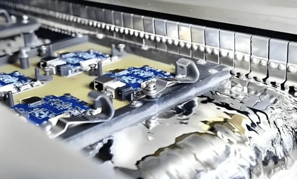
The equipment configuration for wave soldering consists of several integrated subsystems: a conveyor system that transports PCBs through the machine at controlled speeds (typically 0.5-2.5 m/min), a flux application unit, preheat section, solder pot with wave generation mechanism, and cooling system. Modern wave soldering machines often employ dual-wave systems featuring both a turbulent wave to penetrate tightly spaced leads and eliminate shadowing effects, followed by a laminar wave to produce smooth, reliable solder joints. The turbulent wave breaks through surface oxides and provides initial solder deposition, while the laminar wave creates controlled fillets and removes excess solder .
The fundamental principle underlying wave soldering is capillary action, which draws molten solder into the gaps between component leads and PCB pads through surface tension effects. This phenomenon is governed by Jurin’s Law, where the height the liquid solder rises depends on surface tension (γ), contact angle (θ), liquid density (ρ), gravitational acceleration (g), and capillary radius (r). Proper wetting occurs when the solder alloy flows smoothly onto the metal surfaces being joined, creating reliable intermetallic bonds that ensure both electrical conductivity and mechanical strength .
2 PCB Wave Soldering Production Process
The wave soldering process follows a meticulously sequenced series of stages that transform component placements into permanent solder connections. The initial stage involves PCB preparation and fixture installation, where through-hole components are mounted onto the board, often using automated pick-and-place equipment. Proper board support is critical at this stage, as fixtures limit thermal deformation during soldering and protect surface-mount components from being washed off by the solder wave. The prepared PCB then enters the flux application stage, where chemical cleaning agents are precisely applied through spraying, foaming, or selective methods to remove oxides and prevent re-oxidation during heating .
Preheating represents the second critical phase, where the PCB is gradually heated to temperatures between 90-150°C. This serves multiple purposes: activating the flux’s cleaning properties, evaporating solvent carriers from the flux, reducing thermal shock when the board contacts molten solder, and ensuring more uniform temperature distribution across the assembly. Different preheating methods include convection heating (forced hot air), infrared radiation, or combination systems, with the optimal approach depending on board thickness, component density, and thermal mass variations .
The core soldering stage occurs when the preheated PCB passes over the molten solder wave. In dual-wave systems, the board first encounters a turbulent wave that penetrates between closely spaced leads, followed by a laminar wave that finishes the joint formation. Critical parameters at this stage include solder temperature (typically 250-260°C for lead-free alloys), contact time (2-5 seconds), conveyor angle (5-7°), and wave height. The conveyor speed must be precisely controlled—too fast prevents proper wetting, while too slow risks thermal damage to components and board materials .
Table: Key Parameters in Wave Soldering Process
| Process Parameter | Typical Range | Impact on Quality |
|---|---|---|
| Solder Temperature | 245-255°C (lead-free) | Affects wetting quality and intermetallic formation |
| Preheat Temperature | 90-150°C | Activates flux, prevents thermal shock |
| Conveyor Speed | 0.5-2.5 m/min | Determines solder contact time and thermal exposure |
| Wave Height | 4-8 mm | Influences solder penetration and potential bridging |
| Contact Time | 2-5 seconds | Affects joint completeness and component safety |
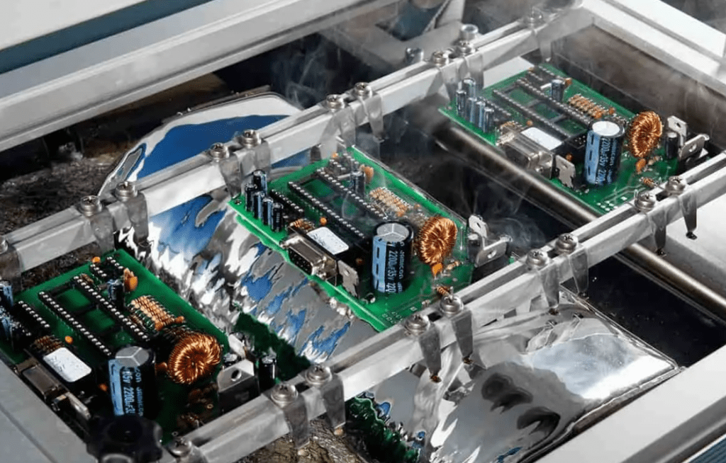
Following solder application, the PCB enters the cooling phase, where controlled solidification of the solder joints occurs. Proper cooling rates (typically 1-2°C per second) prevent thermal stress that could lead to joint cracking or pad lifting. The final stages involve post-soldering cleaning to remove flux residues that could cause corrosion or electrical leakage, followed by comprehensive inspection and quality control using automated optical inspection (AOI), X-ray, or manual methods to identify defects such as bridges, insufficient fill, or cold joints .
3 Types of Wave Soldering
Wave soldering technology has evolved into several distinct configurations to address different manufacturing requirements. The primary classification distinguishes between traditional wave soldering and selective wave soldering systems. Traditional wave soldering processes the entire bottom side of the PCB simultaneously, making it ideal for high-volume production of boards predominantly populated with through-hole components. This approach offers maximum throughput, with modern systems capable of processing 1-2 meters of board length per minute. However, traditional wave soldering presents limitations for mixed-technology boards containing heat-sensitive surface-mount devices, as the entire PCB underside receives equal exposure to molten solder .
Selective wave soldering represents a more targeted approach, using localized solder waves or miniature nozzles to solder specific areas or components without exposing the entire board to high temperatures. This method is particularly valuable for mixed-technology assemblies containing both through-hole and surface-mount components, as it minimizes thermal stress on sensitive devices and reduces solder waste. While selective systems offer superior precision and flexibility, they operate at significantly lower throughput than traditional wave soldering equipment, making them more suitable for low-to-medium volume production or boards requiring specialized processing .
Further classification of wave soldering systems includes single-wave, dual-wave, and multi-wave configurations based on their solder delivery mechanisms. Single-wave systems employ a simple wave profile suitable for basic through-hole assemblies but offer limited capability for complex boards with high component density. Dual-wave systems have become industry standard, combining an initial turbulent wave for penetration with a subsequent laminar wave for joint finishing. Multi-wave systems provide even greater process control for challenging applications, with additional wave configurations that can be tailored to specific component requirements .
The evolution of wave soldering technology has also introduced nitrogen-inerted wave soldering systems, which surround the solder pot with nitrogen gas to minimize oxide formation and improve solder wetting characteristics. This approach is particularly beneficial for lead-free soldering processes, which typically exhibit poorer wetting than traditional tin-lead alloys. While adding to operational costs, nitrogen inerting can significantly reduce defect rates and solder dross formation, particularly in high-volume manufacturing environments .
4 Factors Affecting Wave Soldering Quality
Multiple interrelated factors determine the quality and reliability of wave soldered assemblies, with soldering parameters representing the most directly controllable variables. The solder pot temperature must be precisely maintained—typically 245-255°C for lead-free alloys—as insufficient temperature causes poor wetting and cold joints, while excessive temperature accelerates solder oxidation and may damage components. Similarly, conveyor speed must be optimized to provide adequate contact time with the solder wave (typically 2-5 seconds), as too rapid transit prevents proper capillary action while excessive dwell time increases thermal stress .
PCB design considerations significantly influence wave soldering outcomes. Component spacing must accommodate solder flow without creating bridges, with industry standards typically recommending at least 0.5-1.0mm between adjacent components. Pad and hole size ratios affect solder fill quality, with optimally designed holes providing sufficient clearance for component leads while maintaining appropriate thermal relief patterns. Board layout must also consider the direction of travel through the solder wave, as component orientation can create shadowing effects that prevent proper solder penetration. The copper distribution across the PCB layers affects thermal mass distribution, which must be balanced to ensure uniform heating during preheating and soldering stages .
Material selection constitutes another critical factor, beginning with solder alloy composition. While traditional tin-lead (Sn-Pb) alloys offer excellent wetting properties and lower processing temperatures (220-240°C), environmental regulations have driven widespread adoption of lead-free alternatives such as SAC alloys (Sn-Ag-Cu), which require higher temperatures (245-265°C) and present different wetting characteristics. Flux selection similarly impacts results, with no-clean, water-soluble, and rosin-based variants each offering different activity levels and residue properties. The PCB substrate material itself must withstand soldering temperatures without delamination or excessive warpage, with FR-4 representing the most common choice for its balanced performance characteristics .
Table: Common Wave Soldering Defects and Their Causes
| Defect Type | Primary Causes | Preventive Measures |
|---|---|---|
| Solder Bridging | Insufficient component spacing, excessive solder temperature, incorrect board angle | Optimize design layout, adjust wave height and temperature |
| Cold Solder Joints | Insufficient preheat, low solder temperature, excessive conveyor speed | Thermal profiling, parameter optimization |
| Insufficient Hole Fill | Inadequate flux activity, poor thermal design, incorrect wave contact | Design review, flux selection, wave height adjustment |
| Solder Balls | Moisture absorption, flux volatility, excessive preheat temperature | PCB baking, preheat optimization, flux formulation |
| Icicing | Slow board separation from wave, contamination, incorrect temperature | Adjust conveyor angle, improve cleanliness, temperature control |
Environmental and maintenance factors round out the variables affecting wave soldering quality. Airborne contaminants can compromise flux activity and solder wetting, while temperature and humidity variations affect flux viscosity and performance. Regular equipment maintenance is essential, including solder pot contamination monitoring, wave nozzle cleaning, and preheater efficiency verification. The gradual accumulation of metallic impurities in the solder pot (particularly copper and iron) can alter alloy composition and melting characteristics, necessitating periodic analysis and replenishment with fresh solder .
5 Alternatives to Wave Soldering
While wave soldering remains indispensable for through-hole component assembly, several alternative joining technologies have emerged to address different manufacturing requirements. Reflow soldering represents the primary alternative for surface-mount technology (SMT) assemblies, utilizing solder paste—a mixture of powdered solder and flux—printed onto PCB pads before component placement. The assembled board then passes through a multi-zone reflow oven with precisely controlled temperature profiles that melt the solder particles to form permanent connections. Reflow soldering dominates SMT assembly due to its compatibility with high-density components, precise control over solder volume, and ability to process both sides of a board sequentially. However, it requires different equipment and cannot effectively solder traditional through-hole components without specialized paste formulations and process adaptations .
Selective soldering bridges the gap between wave and reflow processes by targeting specific areas of a PCB for soldering rather than processing the entire board. This approach is particularly valuable for mixed-technology assemblies containing both through-hole and heat-sensitive surface-mount components. Selective soldering systems use programmable nozzles that apply molten solder only to designated through-hole connections, minimizing thermal exposure to adjacent components and the PCB substrate. While significantly slower than wave soldering and requiring more sophisticated programming, selective soldering offers unparalleled precision and is ideal for high-reliability applications where thermal management is critical .
Laser soldering represents a highly precise alternative that directs focused laser energy to specific joint locations, generating localized heating that melts pre-applied solder paste or wire. This non-contact method offers exceptional control with minimal thermal spread, making it ideal for heat-sensitive components, densely packed assemblies, and applications requiring minimal thermal stress. The primary limitations of laser soldering include relatively slow processing speed and higher equipment costs, restricting its economic viability to specialized applications such as medical devices, aerospace systems, and high-value electronics where precision outweighs throughput considerations .
Hand soldering remains relevant for prototyping, rework, and low-volume production where automated processes are impractical. Skilled operators using temperature-controlled irons can address complex geometries and repair defects with flexibility no automated system can match. However, hand soldering suffers from variability in joint quality, higher labor costs, and inconsistent results across operators, making it unsuitable for volume manufacturing. Recent advancements in automated robotic soldering have bridged this gap to some extent, combining the flexibility of manual soldering with the consistency of automation for specialized applications .
6 Advantages and Disadvantages of Wave Soldering
Wave soldering offers distinct advantages that maintain its position in electronics manufacturing decades after its introduction. The process delivers exceptional throughput efficiency, with modern systems processing complete PCBs in 2-5 seconds of solder contact time, translating to production rates exceeding 100 boards per hour depending on size. This high-speed capability makes wave soldering particularly cost-effective for high-volume production, with lower per-unit costs compared to manual or selective soldering methods. The automated nature of wave soldering ensures consistent quality across production runs, minimizing human variability through precise control of temperature, timing, and mechanical parameters .
The process versatility of wave soldering accommodates various PCB designs and component types, particularly through-hole connectors, switches, and large passive components that benefit from the mechanical strength of wave-soldered joints. Modern wave soldering systems can handle board sizes from small modules to large-format panels up to 500mm in width, with appropriate fixture design. The continuous nature of the process allows for seamless integration into inline production systems, connecting automatically with preceding component insertion and subsequent inspection stations in a streamlined manufacturing flow .
Despite these advantages, wave soldering presents significant limitations and disadvantages. The process is predominantly suitable for through-hole components, with limited effectiveness for surface-mount devices that may suffer from displacement, shadowing, or thermal damage. The thermal stress imposed by molten solder exposure (typically 250-260°C) can damage heat-sensitive components and challenge the thermal integrity of PCB materials, particularly in lead-free processes requiring higher temperatures. Design constraints require specific component orientation and spacing to ensure proper solder flow and prevent defects, limiting layout flexibility compared to reflow-based approaches .
The equipment and operational costs of wave soldering systems present another consideration, with sophisticated machines requiring significant capital investment, dedicated facility space, and regular maintenance. Environmental aspects include solder pot management, dross removal, and fume extraction requirements, particularly when using lead-free alloys that generate more oxides. The transition to lead-free soldering has exacerbated some challenges, with higher process temperatures accelerating solder pot corrosion, increasing energy consumption, and generating more dross—the oxidized solder waste that represents both material loss and maintenance burden .
7 Frequently Asked Questions about Wave Soldering
What types of components are best suited for wave soldering?
Wave soldering is primarily optimized for through-hole components, which have leads that insert into plated holes in the PCB. These components include connectors, switches, large capacitors, transformers, and other elements that benefit from the mechanical strength provided by the through-hole mounting method. The wave soldering process efficiently fills the annular space between component leads and PCB holes, creating robust mechanical and electrical connections. Surface-mount components can be wave soldered with appropriate adhesive attachment and process modifications, but this approach has largely been superseded by reflow soldering for SMT devices due to better yield and fewer defects .
Can wave soldering be used for double-sided PCBs?
Yes, wave soldering can process double-sided PCBs, but with specific considerations. Components on the bottom side (facing the solder wave) are soldered directly, while components on the top side must be secured with adhesive to prevent detachment during the soldering process. The approach requires careful thermal management to ensure proper soldering without damaging top-side components, which experience higher temperatures than during reflow processes. For complex mixed-technology boards, many manufacturers combine wave soldering for through-hole components with reflow soldering for surface-mount devices, sometimes adding selective soldering for temperature-sensitive areas .
What are the key factors in wave soldering process setup?
Establishing an optimized wave soldering process requires balancing multiple parameters: solder temperature (245-255°C for lead-free alloys), preheat temperature (90-150°C depending on board thickness and composition), conveyor speed (0.5-2.5 m/min), flux application density, wave height (typically 4-8 mm), and board contact angle (5-7°). The thermal profile must be validated using profiling boards with thermocouples placed at critical locations, particularly areas with high thermal mass or heat-sensitive components. Flux selection should match the cleanliness requirements and solderability challenges of the specific assembly, with no-clean fluxes dominating commercial applications while water-soluble fluxes are preferred for high-reliability systems where post-solder cleaning is feasible .
How can solder defects be minimized in wave soldering?
Defect reduction requires a systematic approach beginning with PCB design optimized for manufacturability, including appropriate component spacing, thermal relief patterns, and solder thief pads where needed. Process control focuses on maintaining stable parameters through regular monitoring and equipment maintenance, including solder pot composition analysis, wave nozzle cleaning, and preheater efficiency verification. Statistical process control (SPC) methods can identify parameter drift before it causes defects, while automated optical inspection (AOI) systems provide immediate feedback for corrective adjustments. Common defects like bridging respond to optimized board orientation, while insufficient hole fill may require increased preheat or flux activity adjustments .
Is wave soldering environmentally friendly?
The environmental impact of wave soldering has improved significantly with the transition to lead-free alloys mandated by RoHS directives worldwide. Modern systems incorporate energy-efficient heaters, improved insulation, and nitrogen inerting systems that reduce dross formation by up to 50%. Flux chemistry has evolved toward halogen-free, low-VOC formulations with reduced environmental impact. However, wave soldering remains an energy-consuming process that generates solder dross, waste flux residues, and requires periodic solder pot maintenance. Best practices include dross recycling programs, efficient fume extraction systems with filtration, and regular maintenance to optimize energy consumption while maximizing solder utilization .
Summary
Wave soldering remains a vital PCB assembly technology nearly seven decades after its introduction, particularly for through-hole components and high-volume production. This automated process delivers unmatched efficiency for mass manufacturing, with continuous improvements maintaining its relevance in modern electronics production. The transition to lead-free soldering has introduced new challenges requiring higher process temperatures and different material compatibility considerations, while technological advancements in selective soldering, nitrogen inerting, and process control have expanded wave soldering capabilities .
The future of wave soldering will likely focus on increased flexibility through hybrid approaches that combine selective soldering capabilities with traditional wave soldering’s throughput advantages. Integration with Industry 4.0 principles will bring smarter monitoring, predictive maintenance, and real-time process adjustment based on incoming board characteristics. Environmental considerations will drive further reductions in energy consumption, dross formation, and material waste, while compatibility with novel PCB materials and components will ensure wave soldering’s continued role in electronics manufacturing for the foreseeable future .


0 Comments