
Introduction
PCB environmental testing refers to a systematic evaluation process that subjects printed circuit boards to simulated conditions replicating their transportation, storage, and operational environments. This testing methodology is crucial for assessing the reliability and durability of PCBs under various stressors, including temperature extremes, humidity fluctuations, mechanical vibrations, and chemical exposures. As electronic devices become increasingly integrated into critical applications across aerospace, automotive, medical, and telecommunications industries, ensuring PCB reliability through comprehensive environmental testing has become a fundamental aspect of product development and quality assurance. These tests help identify potential failure modes before products reach the field, thereby reducing warranty claims and enhancing user safety .
The importance of PCB environmental testing has grown significantly with the miniaturization and increased complexity of electronic systems. Industry data indicates that approximately 35% of electronic device failures are directly attributable to environmental factors, with thermal-related issues accounting for over 55% of these failures. Implementing a robust environmental testing program can reduce field failure rates by up to 40%, significantly improving product reliability and customer satisfaction. International standards organizations such as IPC, IEC, and MIL have established comprehensive testing protocols that provide standardized methodologies for evaluating PCB performance under adverse conditions, ensuring consistency and comparability of results across the industry .

1 What is Environmental Testing for PCBs?
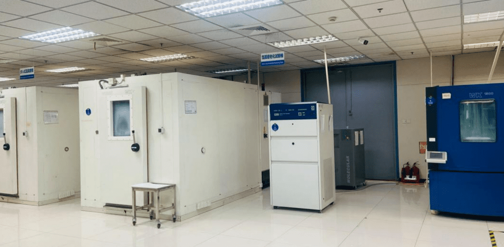
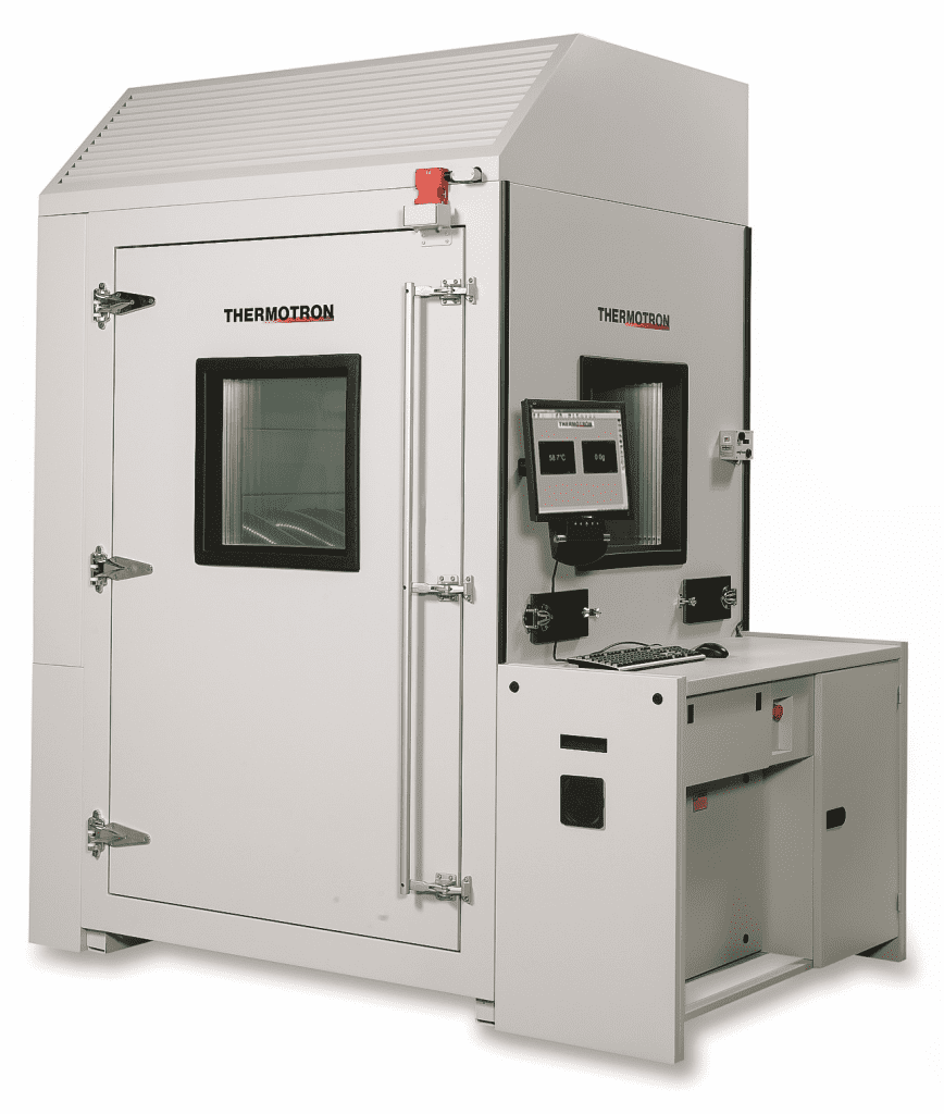
Environmental testing for printed circuit boards comprises a series of structured procedures that expose PCBs to controlled conditions simulating their real-world operating environments. Unlike contamination testing that measures polychlorinated biphenyls in the environment, PCB environmental testing evaluates how circuit boards withstand various stressors including temperature extremes, humidity variations, mechanical shocks, and electromagnetic interference. This form of testing serves as a crucial reliability assessment, verifying whether assembled boards can withstand adverse conditions throughout their expected lifecycle. The tests are conducted in specialized chambers ranging from small benchtop units to walk-in rooms that can simulate everything from desert aridity to tropical humidity .
The fundamental purpose of PCB environmental testing is to identify potential failure mechanisms before products reach the market, thereby reducing field failures and associated costs. These tests accelerate the aging process that would normally occur over years of operation, compressing it into days or weeks of controlled laboratory testing. Through this process, manufacturers can identify weaknesses in materials, design, or workmanship that might not be apparent under normal operating conditions. The testing encompasses electrical, mechanical, and climatic factors that could affect PCB performance, providing comprehensive data for design improvements and quality assurance .
Environmental testing differs significantly from functional testing, which only verifies that a circuit operates correctly under ideal conditions. Instead, environmental testing subjects PCBs to conditions beyond their specified operating ranges to determine their safety margins and failure thresholds. This approach helps establish the operational limits of a design and identifies potential failure modes that could occur under unusual but possible environmental conditions. The results enable engineers to implement corrective actions early in the product development cycle, when changes are least costly and most effective .
2 Why is Environmental Testing Important for PCBs?
Environmental testing is critical for PCBs because it validates their reliability and long-term performance under realistic operating conditions. Electronic devices frequently operate in environments characterized by temperature fluctuations, mechanical vibrations, humidity variations, and other stressors that can lead to premature failure if not properly addressed during design and manufacturing. Without comprehensive environmental testing, PCBs may exhibit unexpected failures in the field, resulting in costly recalls, warranty claims, and damage to brand reputation. Statistical data indicates that PCBs that undergo thorough environmental testing demonstrate up to 40% lower field failure rates compared to untested counterparts, highlighting the significant quality and reliability benefits of these procedures .
The economic implications of environmental testing extend beyond immediate quality assurance to encompass long-term cost savings and risk mitigation. Identifying potential failure modes during the development phase allows for design improvements that are substantially less expensive than post-production modifications or field repairs. Research indicates that addressing design flaws during development is approximately ten times less costly than making changes after production has begun, and a hundred times less expensive than implementing corrections after products have been deployed in the field. Environmental testing also helps manufacturers comply with industry-specific regulations and standards, avoiding potential liability issues and facilitating market access across different regions and industries .
From a technical perspective, environmental testing provides invaluable data on product robustness and safety margins. For instance, thermal cycling tests can reveal coefficient of thermal expansion mismatches between different materials that may lead to solder joint cracking under temperature variations. Vibration testing can identify resonant frequencies that may cause mechanical failures in applications subject to continuous or intermittent motion. Humidity testing can detect potential electrochemical migration issues that might lead to current leakage or short circuits in damp environments. This information enables engineers to optimize designs for specific application requirements, resulting in products that deliver consistent performance throughout their expected service life .
3 PCB Environmental Testing Methods
PCB environmental testing encompasses multiple specialized methodologies that can be broadly categorized into climatic, dynamic, and electromagnetic radiation tests. Climatic testing evaluates a PCB’s response to environmental conditions such as temperature extremes, humidity, corrosive atmospheres, and UV exposure. These tests include temperature resistance assessments that expose boards to extreme temperatures and rapid thermal fluctuations to gauge their thermal endurance. Humidity resistance testing elevates moisture levels to evaluate a PCB’s ability to withstand damp environments, while corrosion resistance testing subjects boards to salt sprays and other corrosive materials to verify their durability in harsh conditions. Additional climatic tests include UV resistance evaluation to check for bleaching and cracking, ingress resistance testing against dust and liquids, and altitude testing that simulates high-elevation conditions including near-space environments .
Dynamic testing focuses on mechanical stresses that occur during shipping, installation, and field application. These tests include vibration and shock assessments that expose PCBs to extreme mechanical disturbances simulating transportation and operational environments. Drop tests evaluate a board’s ability to withstand impact forces from being dropped from specified heights, while mechanical stress testing subjects PCBs to various forces including compression, tension, and shear to validate their structural integrity. These dynamic tests are particularly important for PCBs used in automotive, aerospace, and portable electronics applications where mechanical shocks and vibrations are common .
Table: Major PCB Environmental Testing Methods and Parameters
| Test Category | Specific Methods | Key Parameters | Applicable Standards |
|---|---|---|---|
| Climatic Testing | Temperature cycling, Thermal shock, Damp heat | Temperature range: -40°C to +125°C+, Humidity: 20-95% RH | IEC 60068-2, IPC-TM-650 |
| Dynamic Testing | Vibration, Mechanical shock, Drop test | Frequency range: 5-2000 Hz, Acceleration: up to 1500G | IEC 60068-2-27, MIL-STD-202 |
| Chemical Resistance | Salt spray, Mixed flowing gas | Concentration: 5% NaCl, Exposure: 24-1000 hours | ISO 9227, ASTM B117 |
| Electrical Testing | Insulation resistance, Dielectric strength | Voltage: up to several kV, Resistance: >100 MΩ | IPC-9201, IEC 60112 |
| Accelerated Life Testing | HALT, HASS | Rapid thermal cycling, Multi-axis vibration | IEC 62506, IPC-9701 |
Electromagnetic interference (EMI) testing evaluates a PCB’s susceptibility to electromagnetic radiation from both artificial and natural sources. Conducted emissions tests check a PCB’s susceptibility to EMI transmitted through cables, connectors, and other conductors, while radiated emissions tests assess a board’s ability to withstand electromagnetic energy propagating through space. These tests are crucial for ensuring electromagnetic compatibility (EMC) in increasingly crowded electromagnetic environments, particularly for automotive, medical, and communication equipment where interference can have serious safety implications .
Advanced testing methodologies include Highly Accelerated Life Testing (HALT) and Highly Accelerated Stress Screening (HASS), which subject products to progressively increasing stress levels well beyond their expected operating conditions to identify failure modes and establish design margins. These accelerated tests combine rapid thermal transitions with multi-axis vibration to quickly uncover potential weaknesses in materials, components, or manufacturing processes. While these methods can be controversial due to their aggressive nature beyond standard specifications, they provide valuable insights into product robustness when properly interpreted by experienced engineers .
4 Interpreting PCB Environmental Test Results
Interpreting PCB environmental test results requires a systematic approach that goes beyond simple pass/fail determinations to understand the failure mechanisms and reliability implications. Proper interpretation involves electrical performance monitoring throughout the testing process, physical failure analysis after testing completion, and statistical analysis of results to predict field performance and product lifetime. When failures occur during testing, detailed failure analysis is essential using techniques such as visual inspection, X-ray imaging, scanning electron microscopy (SEM), and energy-dispersive X-ray spectroscopy (EDS) to identify the root cause of failure, whether it be solder joint cracking, conductive anodic filament (CAF) growth, dendrite formation, delamination, or plated through-hole fracture .
The statistical analysis of test data enables reliability prediction and life estimation for the product under expected field conditions. Using statistical methods such as Weibull analysis on temperature cycling data, engineers can estimate the failure rate and mean time to failure (MTTF) of PCBs in actual operating environments. Acceleration factors calculated from test conditions allow the translation of accelerated test results into realistic life expectancy estimates under normal operating conditions. For example, according to the Arrhenius model, for every 10°C increase in temperature, the rate of chemical reactions approximately doubles, correspondingly reducing the product’s expected lifetime. These quantitative analyses provide a scientific basis for design improvements, warranty period establishment, and maintenance schedule development .
Test results are typically categorized into failure, pass, or parameter change classifications, with the latter indicating shifts in characteristics such as capacitance or resistance that may signal impending failure even if the product still meets specifications. The testing expert examines the PCBs after testing to determine the type, extent, and cause of any damage, often creating graphical representations of failure rates to make the results more interpretable. Manufacturers use this environmental testing data to implement quality improvements through design modifications, material upgrades, or manufacturing process adjustments. This continuous improvement cycle helps enhance product reliability and reduce the likelihood of field failures .
5 Environmental Testing in PCB Manufacturing
Environmental testing is integrated throughout the PCB manufacturing process, from material certification to final product validation. During the material selection phase, environmental testing helps verify that base materials, copper foils, solder masks, and other components meet specified requirements for thermal, mechanical, and chemical resistance. Material certification tests might include thermal mechanical analysis (TMA) to measure the coefficient of thermal expansion (CTE) of substrates, ensuring compatibility between different materials in the final assembly. These preliminary tests establish a foundation for product reliability by confirming that the raw materials can withstand the intended operating environment .
Process validation testing assesses the environmental durability of manufacturing processes and identifies potential weaknesses introduced during production. Thermal stress testing, such as the 288°C solder float test, evaluates a PCB’s resistance to soldering heat and reveals potential issues like plated through-hole reliability problems or material delamination. Resistance to electrochemical migration testing assesses the integrity of solder masks, preventing dendrite growth in humid environments. Ionic contamination testing measures the level of ionic residues on PCB surfaces, evaluating the risk of electrochemical migration in humid conditions. These tests provide feedback for process optimization, ensuring manufacturing consistency and environmental stability of the final product .
Table: Key Environmental Testing Points in PCB Manufacturing
| Manufacturing Stage | Test Type | Purpose | Acceptance Criteria |
|---|---|---|---|
| Raw Material Receiving | Thermal Mechanical Analysis (TMA) | Substrate dimensional stability | CTE <3% (z-axis) |
| Inner Layer Fabrication | Chemical Resistance Test | Evaluate photoresist performance | No blistering or peeling |
| After Lamination | Thermal Stress Test | Assess lamination quality and PTH reliability | No delamination or cracking |
| After Solder Mask | Adhesion Test | Evaluate solder mask adhesion | >5B (cross-cut method) |
| After Surface Finish | Solderability Test | Assess pad solderability | Solder coverage area >95% |
| Final Inspection | Temperature Cycling Test | Evaluate overall product reliability | Resistance change <10% |
Environmental testing also includes accelerated stress screening processes applied during manufacturing to eliminate potentially defective products before they reach customers. Common screening methods include temperature cycling (typically 5-20 cycles) and random vibration screening (5-15 minutes duration). These screening stresses exceed normal operating conditions but remain below the product’s demonstrated design limits, aiming to expose early-life failures without significantly consuming the product’s useful life. Effective stress screening improves outgoing quality and reduces field failure rates, particularly for high-reliability applications in automotive, aerospace, and medical industries where failure consequences are severe .
For PCBs destined for specific applications, industry-specific environmental testing is required during manufacturing. Automotive electronics PCBs must undergo chemical resistance testing to simulate exposure to fuels, oils, and cleaning agents encountered in vehicle environments. Aerospace PCBs require low-pressure testing to simulate high-altitude conditions where reduced atmospheric pressure can affect electrical performance. Medical implantable device PCBs need biocompatibility testing to ensure materials are non-toxic and non-irritating. These application-specific tests verify that PCBs can withstand the unique environmental challenges of their intended operating contexts .
6 Circuit Board Environmental Testing Services
Professional circuit board environmental testing services are offered by certified laboratories, independent testing agencies, and specialized departments within large manufacturing companies. These services provide access to advanced testing equipment, technical expertise, and accreditation that may be impractical for individual companies to maintain in-house. When selecting an environmental testing service, key considerations include the laboratory’s accreditation status (such as CNAS or ILAC recognition), testing capabilities (equipment range and precision), and industry-specific experience with similar products and materials. These factors ensure that test results are accurate, reproducible, and recognized by regulatory bodies and customers .
Standard environmental testing services typically include test program development, test execution, data recording, and failure analysis. During the test planning phase, engineers develop a customized testing regimen based on the product’s application field, expected service life, and environmental conditions, selecting appropriate test standards, stress conditions, and acceptance criteria. For example, consumer electronics might follow IEC 60068 series standards, while automotive electronics would require AEC-Q100 compliance. During test execution, technicians follow standardized procedures to ensure result reproducibility and comparability, with comprehensive documentation of test conditions and outcomes .
Modern environmental testing services increasingly offer comprehensive solutions that extend beyond standard testing to include customized testing protocols, rapid cycle testing, and reliability growth services. Customized testing designs protocol specific to a product’s unique usage environment, such as high-pressure testing for deep-sea equipment or sand and dust testing for desert applications. Rapid cycle testing uses higher acceleration factors to significantly reduce test duration, particularly valuable during product development phases. Reliability growth services implement a “test-analyze-fix-retest” approach that systematically identifies and addresses reliability issues through iterative improvement cycles .
Summary
PCB environmental testing represents an essential discipline within electronics manufacturing that validates product reliability, safety, and durability under various environmental stressors. As electronic systems continue evolving toward higher complexity, increased power density, and broader application across diverse industries, the role of comprehensive environmental testing becomes increasingly critical for ensuring long-term performance and customer satisfaction. The systematic approach to environmental testing—from material evaluation through final product validation—provides a scientific basis for design improvements, process optimization, and quality assurance throughout the product lifecycle .
The future of PCB environmental testing points toward more integrated, predictive, and efficient methodologies. Advanced simulation techniques will increasingly complement physical testing, allowing engineers to identify potential failure modes earlier in the design process. Intelligent monitoring systems will provide more comprehensive data collection during tests, while big data analytics and machine learning will enhance failure prediction and root cause analysis. Additionally, growing emphasis on sustainability will drive development of more environmentally friendly testing methods that reduce energy consumption and hazardous material usage while maintaining testing rigor. These advancements will further strengthen the role of environmental testing in delivering reliable electronic products for an increasingly connected world .


0 Comments