
Introduction
High Voltage PCB (Printed Circuit Board) design represents a specialized discipline within electronics engineering focused on creating circuit boards capable of operating at significantly higher voltages than conventional PCBs. While standard PCBs typically handle voltages below 50V, high voltage PCBs are engineered to manage voltages ranging from hundreds to thousands of volts, with some specialized applications reaching tens of kilovolts . This specialized design approach has become increasingly critical in modern electronics, particularly in power conversion systems, renewable energy infrastructure, electric vehicles, medical imaging equipment, and industrial control systems where efficient power management and distribution are paramount .
The importance of high voltage PCB design extends beyond mere functionality to encompass critical safety considerations, reliability requirements, and regulatory compliance. Statistics indicate that approximately 35% of electronic failures in high-power applications can be traced to inadequate voltage isolation or insulation breakdown . Proper high voltage design addresses these challenges through careful attention to creepage and clearance distances, material selection, and layout strategies that prevent arcing, corona discharge, and dielectric breakdown . As electronic systems continue to evolve toward higher power densities and compact form factors, the role of specialized high voltage PCB design has become indispensable for ensuring both performance and safety across numerous industries .
1. What Are High Voltage PCBs?
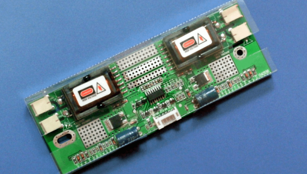
High Voltage PCBs are specialized printed circuit boards engineered to safely and reliably manage electrical potentials significantly higher than those found in conventional electronics. While there’s no universally standardized threshold, the electronics industry generally considers PCBs handling voltages above 100V DC to fall into the high voltage category, with some applications extending to multi-kilovolt ranges . These boards differ fundamentally from standard PCBs through their enhanced safety features, specialized materials, and specific design considerations that prevent electrical breakdown under high potential differences .
The key distinguishing characteristics of high voltage PCBs include significantly increased creepage (surface distance between conductors) and clearance (air distance between conductors) requirements, which are critical for preventing arcing and ensuring long-term reliability . These boards typically employ specialized dielectric materials with higher comparative tracking index (CTI) values, often exceeding 600V, compared to standard FR-4’s 175-300V CTI rating . Additionally, high voltage PCBs incorporate thicker copper traces (typically 2-6 oz/ft² compared to standard 1-2 oz/ft²) to handle increased current flow without excessive heating, and often utilize specialized construction techniques such as isolation slots, protective conformal coatings, and sophisticated thermal management features .
Table: Key Differences Between Standard PCBs and High Voltage PCBs
| Parameter | Standard PCBs | High Voltage PCBs |
|---|---|---|
| Operating Voltage | Typically <50V | >100V, up to kilovolts |
| Creepage/Clearance | Standard spacing | Significantly increased |
| Dielectric Material CTI | 175-300V | >600V preferred |
| Copper Weight | 1-2 oz/ft² | 2-6 oz/ft² (up to 20+ for extreme current) |
| Primary Focus | Signal integrity, density | Safety, isolation, reliability |
| Typical Applications | Consumer electronics, computing | Power supplies, industrial controls, medical equipment |
The fundamental working principle of high voltage PCBs revolves around managing electric field distribution to prevent concentration of electrical stress at any single point. This is achieved through careful control of trace geometry, avoidance of sharp corners, and strategic use of field grading techniques . Additionally, these boards are designed to minimize partial discharge (small electrical discharges that don’t completely bridge the insulation), which can gradually degrade insulation materials over time through a process called electrical treeing . The materials selected for high voltage applications must maintain their dielectric properties under prolonged electrical stress, with dielectric strengths typically exceeding 20kV/mm for standard substrates and reaching 60-100kV/mm for specialized materials like PTFE .
2. Why Design PCBs Specifically for High Voltage Systems?
Designing PCBs specifically for high voltage systems is essential for ensuring safety, reliability, and performance in applications where conventional circuit boards would fail catastrophically. The primary motivation stems from the unique challenges posed by high electrical potentials, including the risk of arc flash events, dielectric breakdown, and corona discharge, which can lead to immediate equipment failure, fire hazards, or safety risks to users . Standard PCB materials and layout practices are insufficient for high voltage applications because they don’t account for the intense electric fields that can cause insulation failure over time, particularly in challenging environmental conditions involving humidity, contamination, or temperature extremes .
From a safety perspective, specialized high voltage PCB design directly addresses the prevention of electrical breakdown through adequate spacing, proper material selection, and appropriate insulation techniques. Industry standards such as IPC-2221 and IEC-60950 provide specific guidelines for clearance and creepage distances based on operating voltage, pollution degree, and material characteristics . For instance, a PCB operating at 1000V in a pollution degree 2 environment typically requires at least 6.3mm of clearance and 12.5mm of creepage distance to ensure safe operation—dimensions far exceeding those found on standard circuit boards . These design considerations become increasingly critical in medical, automotive, and aerospace applications where failure could have severe consequences .
The performance advantages of purpose-designed high voltage PCBs include enhanced thermal management through heavier copper weights, improved reliability under electrical stress, and reduced electromagnetic interference (EMI) through proper layout techniques . High voltage designs also incorporate derating practices—intentionally operating components below their maximum ratings—to extend product lifespan and enhance field reliability . This is particularly important in applications like renewable energy systems and electric vehicle charging infrastructure, where equipment is expected to operate reliably for decades under varying environmental conditions . The economic benefits of proper high voltage design include reduced warranty claims, lower long-term maintenance costs, and compliance with industry regulations that facilitate market access .
3. Advantages and Disadvantages of High Voltage PCB Design
High voltage PCB design offers several significant advantages that make it indispensable for power electronics applications. The most notable benefit is the ability to achieve higher power density within compact form factors, as increased voltage allows for reduced current for the same power level, enabling smaller conductors and components . This principle is particularly valuable in electric vehicle powertrains and renewable energy systems where space and weight constraints are critical design considerations. Additionally, high voltage designs exhibit improved efficiency due to reduced I²R losses (resistive losses proportional to current squared), making them essential for applications where energy conservation is paramount, such as in solar inverters and industrial motor drives .
The use of heavier copper weights (typically 2-6 oz/ft², with extreme applications reaching 20+ oz/ft²) in high voltage PCBs provides enhanced current-carrying capacity, superior thermal management through better heat dissipation, and increased mechanical strength at connector sites and plated through-holes . This construction approach also enables reduced system complexity in many applications—for instance, in power transmission systems, higher voltages minimize voltage drop over distance, reducing the need for additional regulation stages . The inherent safety focus of high voltage design principles results in more robust products capable of withstanding harsh operating environments, including those with wide temperature fluctuations, mechanical vibration, and contamination concerns .
Despite these advantages, high voltage PCB design presents several significant challenges that must be carefully managed. The most prominent disadvantage is increased cost due to specialized materials, more complex manufacturing processes, and stringent testing requirements . High voltage-grade materials with superior dielectric properties typically cost 30-50% more than standard FR-4, and the fabrication process requires greater precision, particularly in layer-to-layer registration and controlled impedance requirements . Additionally, the design cycle is often lengthier due to the need for more extensive simulation, prototyping, and validation testing to ensure safety and reliability .
Table: Comprehensive Analysis of High Voltage PCB Design Trade-offs
| Aspect | Advantages | Disadvantages |
|---|---|---|
| Performance | Higher power density, reduced resistive losses, improved efficiency at equivalent power | Increased electromagnetic interference (EMI), stricter signal integrity requirements |
| Thermal Management | Better heat dissipation through heavier copper, integrated thermal management features | Additional cooling requirements due to higher power dissipation, complex thermal design |
| Reliability | Enhanced safety margins, robust construction, longer lifespan under electrical stress | More complex failure modes (partial discharge, corona), stringent material requirements |
| Cost Structure | Reduced system-level costs in high-power applications, optimized power delivery networks | Higher PCB manufacturing costs (20-50% premium), specialized components, extensive testing |
| Design Complexity | Integration of power and control functions, optimized board space utilization | Lengthy design cycles, sophisticated simulation requirements, specialized expertise needed |
Other significant drawbacks include limited component availability,
as not all electronic components are rated for high voltage operation, potentially restricting design options . The physical size of high voltage PCBs is often larger than their low-voltage counterparts due to increased spacing requirements, running counter to the general trend of electronics miniaturization . Additionally, these designs require specialized expertise in both design and manufacturing, with a steep learning curve that can present barriers to entry for organizations new to high voltage applications . The testing and certification process is also more rigorous, often requiring sophisticated equipment such as hipot testers and partial discharge detection systems, further adding to development time and cost .
4. How to Select Materials for High Voltage PCBs
Material selection is a critical determinant of performance and reliability in high voltage PCB design, with considerations extending far beyond those of conventional circuit boards. The primary factor in material selection is dielectric strength—the maximum electric field a material can withstand without breaking down, typically measured in kilovolts per millimeter (kV/mm) . Standard FR-4 material offers dielectric strength ranging from 20-40kV/mm, while specialized materials like polyimide (40-70kV/mm) and PTFE (60-100kV/mm) provide significantly higher performance for demanding applications . The selected material must maintain its insulating properties not only under initial testing but throughout the product’s operational life, resisting degradation from partial discharge, thermal cycling, and environmental exposure .
The Comparative Tracking Index (CTI) represents another crucial material parameter, measuring a material’s resistance to surface tracking (the formation of conductive paths along the surface due to contamination and humidity) . For high voltage applications, materials with CTI ratings of 600V or higher are preferred, as they allow for reduced creepage distances while maintaining safety—a significant consideration for compact designs . Standard FR-4 typically has a CTI between 175V and 300V, necessitating alternative materials like specialized epoxy composites or ceramic-filled laminates for applications where space constraints conflict with safety spacing requirements . Materials with higher CTI ratings are particularly important in applications prone to contamination or operating in high-humidity environments .
Thermal management properties must be carefully evaluated, including thermal conductivity coefficient, glass transition temperature (Tg), and coefficient of thermal expansion (CTE) . High voltage circuits often generate significant heat, requiring materials with adequate thermal conductivity to transfer heat away from critical components. For applications with significant temperature fluctuations, materials with high Tg (typically >170°C for high voltage applications) and controlled CTE ensure dimensional stability and prevent delamination or via cracking . In extreme thermal environments, metal-clad substrates (such as aluminum or copper base materials) or ceramic-based substrates may be necessary to manage heat effectively .
The selection process should also consider mechanical properties such as flexural strength, especially for applications subject to vibration or mechanical stress . For flexible high voltage circuits, polyimide materials offer excellent thermal stability and mechanical flexibility. Manufacturing compatibility is another practical consideration—some high-performance materials require specialized drilling parameters, lamination cycles, or surface treatment processes that may impact manufacturability and cost . Finally, regulatory compliance and cost-effectiveness must be balanced against performance requirements, with material selection often involving trade-offs between ideal properties and practical constraints .
5. Types of High Voltage Printed Circuit Boards
High voltage printed circuit boards can be categorized into several distinct types based on their construction methodology, layer count, and material flexibility, each suited to specific applications and operating environments. The most fundamental classification is based on layer count and configuration, with the main categories being single-sided, double-sided, and multi-layer boards . Single-sided high voltage PCBs feature conductive traces on only one side of the substrate, representing the simplest and most cost-effective construction suitable for basic high voltage circuits with low component density . Double-sided boards contain copper layers on both sides of the substrate, connected by plated-through holes (vias), allowing for more complex interconnections and higher component density . Multi-layer high voltage PCBs incorporate three or more copper layers separated by insulating dielectric materials, enabling complex, high-density interconnections required for advanced systems such as industrial motor drives, power inverters, and medical imaging equipment .
Beyond layer count, high voltage PCBs are further classified by their mechanical properties and flexibility. Rigid high voltage PCBs use solid substrate materials that provide structural stability but cannot be bent or flexed during use . Flexible high voltage PCBs employ bendable substrate materials such as polyimide, allowing them to conform to unusual shapes or withstand repeated flexing in applications like medical equipment, aerospace systems, and certain automotive applications . Rigid-flex high voltage PCBs combine rigid and flexible sections in a single structure, providing both stable mounting platforms for components and flexible interconnections between rigid sections, particularly valuable in aerospace, medical, and military applications where reliability, space savings, and three-dimensional packaging are critical requirements .
Metal-core PCBs represent a specialized category designed for applications requiring exceptional thermal management, such as high-power LED lighting, power converters, and automotive systems . These boards incorporate a metal baseplate (typically aluminum or copper) to provide enhanced heat dissipation away from critical components . The metal core is insulated from the circuit layer by a thermally conductive but electrically insulating dielectric layer, allowing the metal to function as a heat spreader while maintaining electrical isolation . This construction is particularly advantageous for high power density designs where concentrated heat generation could compromise reliability or performance .
Table: High Voltage PCB Types and Their Characteristics
| PCB Type | Layer Structure | Key Features | Typical Applications |
|---|---|---|---|
| Single-Sided | Conductive layer on one side only | Simple design, lowest cost, limited complexity | Basic power supplies, simple controls |
| Double-Sided | Conductors on both sides, connected by vias | Medium complexity, better component density | Power converters, industrial controls |
| Multi-Layer | Three or more conductive layers | High component density, complex interconnections | Motor drives, inverters, medical imaging |
| Rigid-Flex | Combination of rigid and flexible sections | 3D packaging, vibration resistance, space-saving | Aerospace, military, medical devices |
| Metal-Core | Metal baseplate for thermal management | Excellent heat dissipation, high power handling | Power electronics, LED lighting, automotive |
Specialized high voltage PCB types address specific application requirements that standard constructions cannot meet. High-frequency high voltage PCBs use specialized low-loss dielectric materials with controlled dielectric constants to maintain signal integrity at microwave and millimeter-wave frequencies, essential for RF power amplifiers and communication systems . Heavy copper PCBs employ extreme copper weights (up to 20 oz/ft² or more) to handle very high currents alongside high voltages, commonly found in power distribution systems and high-current motor controllers . Hybrid construction PCBs combine different technologies and materials on a single board, such as thick-film ceramic substrates for high voltage sections combined with standard FR-4 for control circuits, optimizing performance while containing costs . Each PCB type offers distinct advantages and involves specific design considerations, with selection depending on the electrical, thermal, mechanical, and cost requirements of the target application .
6. How Are Bare High Voltage Circuit Boards Manufactured?
The manufacturing process for bare high voltage circuit boards is a precision-oriented sequence that demands strict adherence to specialized procedures to ensure dielectric integrity and long-term reliability. The process begins with material preparation and inner layer fabrication, where copper-clad laminate sheets are cut to the required panel size and cleaned to remove contaminants . For multi-layer boards, the inner layers undergo a pattern transfer process using photoresist and UV exposure through a photomask containing the circuit pattern . The exposed copper is then etched away, leaving only the desired circuit pattern protected by the hardened photoresist. This stage requires exceptional precision, as any imperfections in the inner layers can create potential failure points in the finished board .
Layer alignment and lamination represent critical phases for multi-layer high voltage boards. The inner layer cores, prepreg sheets (partially cured dielectric material), and copper foil for outer layers are stacked in precise alignment according to the designed layer sequence . This stack undergoes lamination under high temperature (typically 180-200°C) and pressure (200-300 psi), causing the prepreg to flow and bond the layers into a solid panel . The lamination process must be carefully controlled to prevent voids, delamination, or resin starvation that could compromise the dielectric strength between layers . For high voltage applications, the dielectric thickness between layers is typically increased, and materials with higher glass transition temperatures (Tg) are often employed to enhance thermal and electrical stability .
Drilling and via formation require special attention in high voltage PCBs due to the potential for creating weak points in the dielectric barrier. High-precision drilling machines create holes for vias and component leads, with the process parameters carefully controlled to minimize drilling-induced defects that could lead to partial discharge or breakdown . The drilled holes are subsequently metallized through electrodes copper deposition followed by electroplating to establish electrical connections between layers . For high voltage designs, via tenting (covering vias with solder mask) is often employed to increase surface creepage distance, and additional clearance is maintained around holes connecting to high voltage nets .
The final manufacturing stages include outer layer processing, solder mask application, and surface finish. Outer layers undergo a similar pattern transfer process as inner layers, after which a solder mask is applied to protect the copper traces and prevent solder bridging . For high voltage boards, the solder mask must have excellent dielectric properties and adhesion characteristics, with complete coverage ensured in high field strength areas . The surface finish is then applied to protect exposed copper pads and ensure solderability, with common choices for high voltage applications including ENIG (Electroless Nickel Immersion Gold) and immersion silver, which provide flat, reliable surfaces . Throughout the process, rigorous quality control measures, including automated optical inspection (AOI) and electrical testing, verify that the finished bare board meets all specifications before component assembly .
7. High Voltage PCB Design Considerations
High voltage PCB design requires meticulous attention to numerous factors that differ significantly from conventional circuit board design. The foremost consideration is clearance and creepage distance management, which directly impacts the board’s ability to prevent electrical arcing and surface tracking . Clearance refers to the shortest air path between two conductive elements, while creepage is the shortest path along the surface of the insulation material . These parameters must be determined based on the operational voltage (including transients), pollution degree of the operating environment, altitude, and the comparative tracking index (CTI) of the base material . Standards such as IPC-2221 and IEC-60950 provide detailed guidelines—for example, at 1000V in a pollution degree 2 environment, typical requirements might be 6.3mm clearance and 12.5mm creepage . Designers must incorporate substantial safety margins beyond these minimums to account for manufacturing tolerances, long-term material degradation, and unexpected environmental conditions .
Copper trace design requires careful consideration of width, thickness, and geometry to manage both current-carrying capacity and electric field distribution . Trace widths must be sufficient to handle the expected current without excessive heating, with a general guideline of at least 1mm per 100V to prevent surface tracking . Sharp corners and acute angles in traces create points of high electric field concentration and must be replaced with curved traces or angles no sharper than 45 degrees to minimize field intensification . Current density calculations should maintain conservative derating factors, with many high voltage designs limiting traces to 10-15A/mm² compared to the 20-30A/mm² common in low voltage designs . Additionally, thermal management considerations may necessitate thicker copper (2-6 oz/ft²) than typically used in standard PCBs, particularly in power conversion sections where I²R losses generate significant heat .
Table: Key High Voltage PCB Design Parameters and Recommendations
| Design Parameter | Consideration | Recommendation |
|---|---|---|
| Clearance/Creepage | Prevents arcing and tracking | Follow IPC-2221/IEC-60950 with safety margins; increase for pollution/humidity |
| Trace Geometry | Manages current and electric fields | Minimal 45° angles; curved traces preferred; adequate width for current with derating |
| Dielectric Material | Withstands electric stress | High CTI (>600V), high dielectric strength materials; consider polyimide/PTFE for extreme voltages |
| Layer Stackup | Manages interlayer stress | Increased dielectric thickness between high voltage layers; shield layers when needed |
| Via Design | Prevents breakdown at transitions | Tent vias with solder mask; avoid via-in-pad for high voltage; thermal relief patterns |
| Component Placement | Facilitates proper spacing | Group by voltage level; isolate high and low voltage areas; consider maintenance access |
Material selection critically influences the performance and reliability of high voltage PCBs . Standard FR-4 may be adequate for lower high voltage applications (up to several hundred volts), but specialized materials with higher comparative tracking index (CTI) and dielectric strength are necessary for more demanding applications . Materials like polyimide, PTFE, and ceramic-filled composites offer superior performance but at increased cost and with different processing requirements . The dielectric constant (Dk) and dissipation factor (Df) of materials become increasingly important at higher frequencies, influencing impedance control and signal integrity in mixed-signal high voltage designs . Additionally, the thermal properties of materials, including thermal conductivity and coefficient of thermal expansion (CTE), must be compatible with the operating environment to prevent delamination or cracking under thermal cycling .
Advanced design techniques for high voltage PCBs include implementing isolation strategies such as slotting between high and low voltage sections, using conformal coatings to enhance surface insulation resistance, and incorporating guard rings to control electric field distribution . Thermal management requires special attention, potentially incorporating thermal vias, heatsinks, and metal-core substrates to dissipate heat generated by power components . For mixed-signal designs, proper grounding schemes and shielding are essential to prevent noise coupling from high voltage switching sections to sensitive low voltage circuitry . Finally, design for manufacturability (DFM) considerations must be integrated early in the process, accounting for material availability, fabrication tolerances, and testability to ensure a robust, producible design .
8. High Voltage PCB Applications
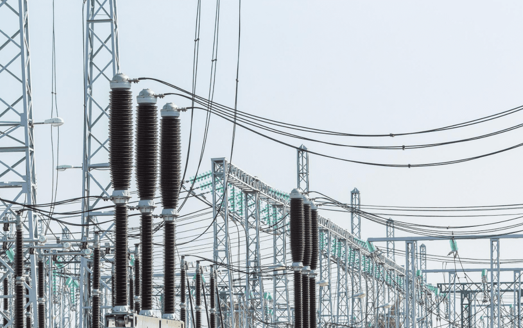
High voltage PCBs serve critical functions across diverse industries where efficient power management, conversion, or distribution is required. The renewable energy sector represents a major application area, with high voltage boards forming the core of solar microinverters, wind turbine control systems, and grid-tie equipment that interfaces renewable sources with traditional power infrastructure . In solar energy systems, high voltage PCBs in inverters must efficiently convert the direct current (DC) from photovoltaic panels (often at 600-1500V) to grid-compatible alternating current (AC) while withstanding environmental challenges including temperature extremes, humidity, and potential contamination . These applications demand exceptional reliability, with design lifespans often exceeding 20 years of continuous operation .
The automotive and transportation sector has emerged as a significant growth area for high voltage PCBs, particularly with the rapid adoption of electric and hybrid vehicles . These boards are integral to battery management systems (BMS), onboard chargers, DC-DC converters, and motor drive electronics that operate at voltages ranging from 400V to 800V in modern electric vehicles . Automotive applications present unique challenges, including extreme temperature cycling, vibration, and stringent safety requirements, necessitating robust designs with enhanced thermal management and conformal coatings for protection against contaminants . High voltage PCBs in transportation applications must comply with industry-specific standards such as ISO 26262 for functional safety and AEC-Q100 for component reliability .
Medical equipment constitutes another critical application domain for high voltage PCBs, where reliability and safety are paramount . Medical imaging systems including X-ray generators, computed tomography (CT) scanners, and magnetic resonance imaging (MRI) systems employ high voltage PCBs to generate and control the precise high voltages required for operation—in some cases exceeding 100kV . Therapeutic medical devices such as electrosurgical units and defibrillators also rely on high voltage PCB technology to deliver controlled energy doses while ensuring patient and operator safety through reinforced insulation and comprehensive safety systems . Medical applications typically require compliance with stringent regulatory standards such as IEC 60601-1, which specifies creepage, clearance, and isolation requirements for medical electrical equipment .
Table: High Voltage PCB Applications by Industry and Requirements
| Industry | Typical Applications | Voltage Range | Key Requirements |
|---|---|---|---|
| Renewable Energy | Solar inverters, wind turbine controls, grid-tie equipment | 600V-1500V | High efficiency, long-term reliability, environmental resistance |
| Automotive/Transportation | EV powertrains, charging systems, battery management | 400V-800V (in vehicles); up to 1000V (charging) | Thermal cycling resistance, vibration endurance, automotive safety standards |
| Medical Equipment | X-ray systems, MRI, defibrillators, electrosurgical units | Several kV to >100kV | Patient safety, reliability, compliance with medical device standards |
| Industrial Equipment | Motor drives, power supplies, laser systems, automation controls | 240V-1000V+ | Robustness, extended temperature range, industrial safety standards |
| Aerospace/Defense | Avionics, radar systems, power distribution, communication equipment | 270V-1000V+ | Extreme environment operation, military standards, high reliability |
Industrial applications for high voltage PCBs include motor drives for industrial machinery, power supplies for automation equipment, high-power laser systems, and plasma generation equipment . These applications often involve harsh operating environments with elevated temperatures, conductive contaminants, and sustained operational demands that necessitate particularly robust designs . Industrial high voltage PCBs frequently incorporate enhanced insulation systems, conformal coatings for protection against industrial atmospheres, and sophisticated thermal management to ensure reliable operation over extended periods . The aerospace and defense sectors utilize high voltage PCBs in applications including aircraft power distribution systems, radar and communication equipment, and defense systems where reliability under extreme conditions is critical . These applications often require compliance with military specifications (such as MIL-PRF-31000) and specialized materials capable of withstanding wide temperature ranges, high vibration levels, and other challenging environmental conditions .
Summary
High voltage PCB design represents a specialized discipline that balances electrical safety, thermal management, and reliability considerations distinct from conventional circuit board design. The unique challenges of managing elevated potentials—from hundreds to thousands of volts—require meticulous attention to clearance and creepage distances, sophisticated material selection, and careful layout strategies to prevent dielectric breakdown, arcing, and surface tracking . As electronic systems continue to evolve toward higher power densities and increased efficiency demands, the role of specialized high voltage PCB design has become increasingly critical across industries including renewable energy, electric transportation, medical imaging, and industrial automation .
The future of high voltage PCB technology points toward continued innovation in materials, manufacturing techniques, and design methodologies. Emerging trends include the development of nano-composite dielectric materials with enhanced thermal and electrical properties, embedded component technology that reduces surface arcing risks, and additive manufacturing approaches that enable more complex high voltage structures . The adoption of wide bandgap semiconductors (SiC and GaN) is pushing operational frequencies and temperatures higher, creating new design challenges and opportunities for improved power conversion efficiency . As sustainability concerns grow, the industry is also developing more environmentally friendly materials, including bio-based dielectrics and halogen-free flame retardants, without compromising performance . These advancements will continue to enable new applications while improving the reliability, efficiency, and safety of high voltage electronic systems across all sectors .


0 Comments