
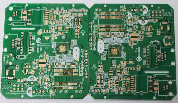
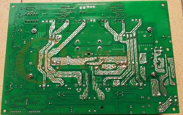
Copper clad PCB are one of the most fundamental and critical components of modern electronic devices. From smartphones and computers to industrial automation equipment and automotive electronics, almost all electronic products rely on them.
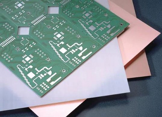
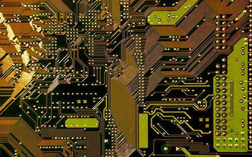
These circuit boards use insulating materials such as fiberglass or resin (common types include FR4, CEM-1, and phenolic resin) as the substrate, and are coated with a layer of high-purity copper foil on one or both sides. The copper layer forms conductive paths through etching or machining, enabling connections and signal transmission between electronic components.
The copper layer not only provides excellent conductivity but also excellent heat dissipation, which is crucial for the stability of the circuit system. During the design phase, engineers must select the appropriate copper clad laminate (CCL) based on the application environment to balance performance and cost. Thindry employs advanced copper lamination technology to ensure high reliability, high conductivity, and excellent thermal stability in its products.
What is a Copper Clad PCB?
In the PCB manufacturing industry, we often hear the term “copper clad laminate.” What exactly does it mean?
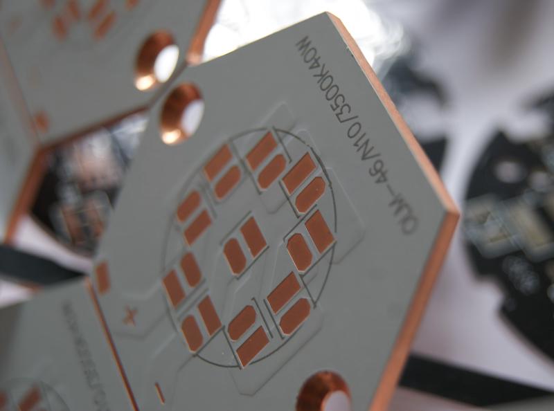
A copper clad PCB refers to a circuit board with a copper foil layer laminated onto its substrate. This copper foil provides the necessary conductive path and protects the substrate from environmental influences.
Copper clad laminate is the fundamental material for manufacturing printed circuit boards. It uses fiberglass cloth or wood pulp paper as reinforcement, impregnates it with resin, and then laminates it with copper foil on one or both sides. This material combines excellent mechanical strength, electrical properties, and dimensional stability, making it a key foundation for achieving high-quality PCB manufacturing.
Common Methods for Designing and Manufacturing Copper Clad PCB
Copper clad PCB are one of the most common and critical basic components in the electronics industry. The design of their copper layer directly affects the circuit board’s conductivity, heat dissipation, and electromagnetic compatibility. In the PCB design and manufacturing process, the design of the copper layer is a key step in ensuring product performance and stability. Below, we will introduce several commonly used copper layer design methods to help you better understand and apply these techniques.
- 1. Reasonable Copper Coverage Area
The copper layer coverage ratio significantly affects the overall performance of the circuit board. To ensure stable signal transmission and good heat dissipation, the copper area is usually required to be no less than 30% of the total PCB area. Sufficient copper not only helps reduce impedance but also improves the stability of power and ground planes.
- 2. Optimized Grounding Design
A reasonable grounding layout is crucial for reducing electromagnetic interference. During the design phase, ensure that all ground wires are connected to a unified grounding point, forming a continuous ground plane, thereby effectively improving the circuit’s anti-interference performance and signal integrity.
- 3. Appropriate Trace Width and Spacing
The width and spacing of traces also affect the reliability and transmission efficiency of the circuit. Designers need to determine the line width reasonably according to the actual current and voltage requirements, and maintain sufficient spacing to avoid crosstalk or breakdown problems between adjacent lines.
What are the applications of CCL?
- 1. Concept and Development Overview of CCL
CCL are composite electronic materials made by hot-pressing copper foil with an insulating substrate (such as epoxy resin glass cloth, paper, or other composite materials). They are one of the fundamental materials for PCB and hold an irreplaceable position in the electronics and information industry. With the rapid development of semiconductor technology, communication equipment, and intelligent manufacturing, the performance of CCL has continuously improved, and their application areas have expanded from traditional electronic products to high-end industries such as automotive electronics, 5G communication, industrial control, and aerospace.
- 2. Applications of CCL in Circuit Board Manufacturing
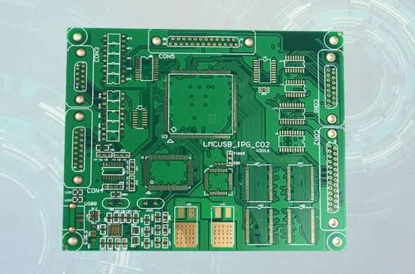
CCL play a crucial role in circuit board manufacturing. They not only serve as a carrier for circuit conductors but also determine the mechanical strength, thermal conductivity, and stability of the circuit board. Through etching, drilling, electroplating, and printing processes, precise circuit patterns can be formed on CCL to meet the design requirements of different electronic devices. High-quality CCL possess excellent conductivity, heat resistance, and dimensional stability, making them key materials for ensuring reliable circuit board performance and long lifespan.
- 3. Applications of CCL in the Manufacturing of Other Electronic Components
Besides printed circuit boards, copper clad laminates are widely used in the manufacturing of various electronic components and modules. For example, in semiconductor packaging substrates, power modules, antenna boards, sensors, and radio frequency components, copper clad laminates, with their excellent conductivity, dielectric properties, and thermal management capabilities, can significantly improve the operating efficiency and stability of electronic devices. As electronic devices develop towards higher frequencies, higher speeds, and miniaturization, the demand for high-performance copper clad laminates continues to grow.
Choosing a Copper Clad Laminate (CCL)
The selection of copper clad laminates (CCL) is crucial in PCB manufacturing. Manufacturers typically evaluate and select based on requirements such as electrical performance, mechanical strength, chemical properties, and application environment.
- 1.Dimensional Requirements
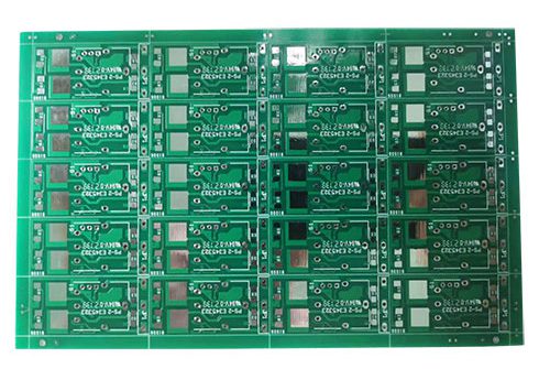
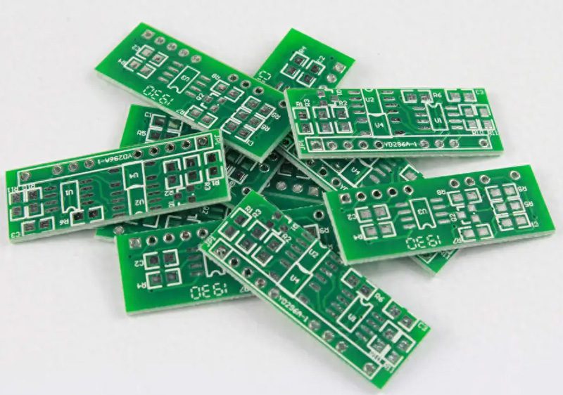
As the base material for printed circuit boards, the dimensions of the copper clad laminate must strictly match the design requirements. To improve production efficiency, manufacturers often panelize smaller PCB. Key dimensional parameters include length, width, diagonal deviation, and warpage, which directly affect the accuracy and assembly quality of subsequent processes.
- 2.Appearance Quality
During production and handling, defects such as dents, scratches, bubbles, pinholes, resin spots, or wrinkles may appear on the surface of the copper clad laminate. These defects not only affect the appearance of the finished product but may also reduce the reliability of the PCB. Therefore, a high-quality copper clad laminate should have a smooth, clean surface without obvious defects.
- 3.Physical Properties
High-quality copper clad laminates should possess good dimensional stability, bending strength, peel strength, heat resistance, and stamping performance. These performance indicators determine whether the PCB can maintain structural stability and controllable deformation during manufacturing and assembly.
- 4.Electrical Performance
The electrical characteristics of copper-clad laminates directly determine the signal transmission performance of the circuit board. Designers must pay close attention to parameters such as dielectric constant (Dk), dielectric loss tangent (Df), insulation resistance, arc resistance, and dielectric breakdown voltage when selecting materials to ensure excellent signal integrity and anti-interference capabilities.
- 5.Chemical and Thermal Properties
For different application environments, copper-clad laminates must possess good chemical corrosion resistance, flame retardancy, and a low Z-axis coefficient of thermal expansion (CTE). Simultaneously, their glass transition temperature (Tg) and dimensional stability must meet the requirements of high-temperature soldering and long-term operation.
- 6.Environmental Adaptability
Finally, the water absorption rate and environmental stability of copper-clad laminates are also important selection criteria. Low water absorption not only prevents material expansion and deformation but also maintains long-term stability of electrical performance.
How are CCL classified?
Copper clad laminates (CCL) can be classified into several types according to different standards, each corresponding to different performance and application scenarios.
- 1. Classification by Mechanical Rigidity
Based on the mechanical rigidity of the conductive layer, CCL can be divided into rigid CCL (such as FR-4, CEM-1, etc.) and flexible CCL. Rigid PCB rely on rigid substrates, while flexible PCB use flexible materials; rigid-flex PCB use both substrates, combining structural strength and flexibility.
- 2. Classification by Insulation Material and Structure
Based on the material and structure of the insulation layer, CCL can be divided into organic resin substrates (such as FR-4, CEM-3), metal-based CCL (such as aluminum-based, copper-based), and ceramic-based CCL. Different substrates correspond to different heat dissipation performance and dielectric properties.
- 3. Classification by Thickness
Based on the thickness of the conductive layer, CCL can be divided into standard thickness boards (thickness ≥ 0.5mm) and thin boards (thickness < 0.5mm). It is important to note that the copper foil thickness is not included in the conductive layer thickness.
- 4. Classification by Reinforcing Material
Based on the reinforcing material, CCL can be classified into glass fiber cloth substrates (such as FR-4, FR-5), paper substrates (such as XPC), and composite substrates (such as CEM-1, CEM-3). Glass fiber cloth substrates offer higher strength and stability and are often used in high-reliability circuit designs.
- 5. Classification by Resin Type
Based on the insulating resin used, CCL can be classified into epoxy resin-based (such as FR-4, CEM-3) and phenolic resin-based (such as FR-1, XPC). Epoxy resin-based boards offer superior performance and wider applications, while phenolic resin-based boards are lower in cost and suitable for mid-to-low-end products.
How many types of copper clad laminates are there?
Copper clad laminates (CCL) can be classified in several ways, such as size, thickness, mechanical properties, structural form, insulating material, reinforcing material, resin type, and overall performance.
Generally speaking, copper clad laminates can be divided into two main categories: rigid copper clad laminates and flexible copper clad laminates.
Rigid copper clad laminates: These use fiberglass cloth or paper-based materials as reinforcement and can be further subdivided into various types depending on the material combination. Some rigid copper clad laminates possess high flame retardancy or special electrical properties and are often used in high-reliability electronic devices.
Flexible copper clad laminates: These use flexible materials as a substrate and are characterized by their bendability and thinness. They are widely used in portable electronic devices and flexible connections. Common types include:
Non-flame retardant polyester film (PET)
Flame retardant polyester film (FR-PET)
Flame retardant-containing polyimide (FR-PI)
Flame retardant-free polyimide (Non-FR PI)
Thin fiberglass cloth base material
Different types of copper clad laminates have their own advantages in heat resistance, mechanical strength, flexibility and electrical properties. When making a selection, the actual application requirements should be considered comprehensively.
How to Solve Problems with Copper Clad PCB Laminates?
Quality problems are almost unavoidable in the PCB manufacturing process, and these problems are often closely related to the material properties of copper clad laminates (CCL). In practice, even with well-developed and strictly implemented CCL technical specifications, there is a lack of unified standards to clearly define which tests can effectively determine whether the CCL is the root cause of the problem.
When problems related to CCL occur, they should be recorded promptly and included in the material specifications for subsequent tracking and improvement. Failure to improve technical specifications can easily lead to continuous fluctuations in production quality, even resulting in product scrap. Differences in material batches or inconsistencies in pressing process parameters (such as pressure and temperature) are the main causes of quality problems.
Because most manufacturers lack complete records of each batch of materials and process parameters (such as pressing pressure, resin batch, copper foil batch number, and curing cycle), problems such as PCB warping often occur during continuous production, leading to component damage and wasted labor.
Therefore, establishing a comprehensive material traceability system is crucial. Through batch traceability and production data recording, PCB laminate manufacturers can quickly locate the source of problems and ensure the consistency and stability of each batch of products. Only by maintaining close quality control collaboration with copper clad PCB suppliers can we effectively reduce long-term production risks and improve overall product reliability and production efficiency.
Applications and Challenges of Copper Clad PCB in Other Fields
With the continuous advancement of electronic and communication technologies, the application areas of copper clad PCB are rapidly expanding, and their performance requirements are becoming increasingly stringent. In emerging fields, copper clad PCB not only undertake the basic functions of circuit connection and signal transmission, but also play a crucial role in high-frequency, high-speed, and high-reliability scenarios.
- 1. New Requirements for Copper Clad PCB from 5G Communication
With the popularization of 5G communication technology, the demands of communication equipment for high-speed signal transmission, low loss, and thermal stability have significantly increased. As a core circuit material, the performance of copper clad PCB directly affects signal integrity and system reliability. To adapt to 5G base stations, RF modules, and high-speed interconnect applications, copper clad PCB must possess higher conductivity, lower dielectric loss, better dimensional stability, and thermal management capabilities. Furthermore, the requirements for material dielectric constant consistency, surface flatness, and resistance to damp heat are becoming more stringent.
- 2. New Opportunities and Challenges Brought by Millimeter-Wave Communication Technology
Millimeter-wave communication, as an important development direction for 5G and the future 6G, places higher standards on the dielectric performance and processing precision of copper clad PCB. Millimeter-wave signals are characterized by high frequency and high loss, necessitating the use of high-quality copper clad PCB with low dielectric constants and low loss tangents to ensure high-speed and stable signal transmission. Simultaneously, the thermal conductivity, dimensional stability, and lamination accuracy of materials are particularly critical in millimeter-wave antennas and radar systems. The development of high-frequency, high-performance copper clad PCB is becoming a crucial link in driving performance improvements in millimeter-wave communication equipment.
- 3. Future Development Trends of Copper Clad PCB
Looking ahead, the copper clad PCB industry will continue to evolve towards high-frequency, high-speed, environmentally friendly, energy-saving, and multifunctional directions. High-performance copper clad PCB will play an increasingly important role in 5G communications, automotive electronics, artificial intelligence, new energy, and aerospace. At the same time, green and environmentally friendly copper clad boards will become the market mainstream. With the continuous advancement of new material technologies, precision machining, and intelligent manufacturing processes, copper clad PCB will demonstrate broad application prospects and development potential in more high-end fields.


0 Comments