
Introduction
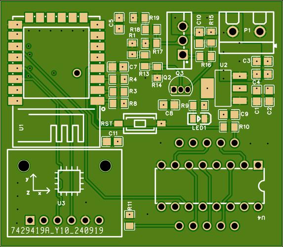
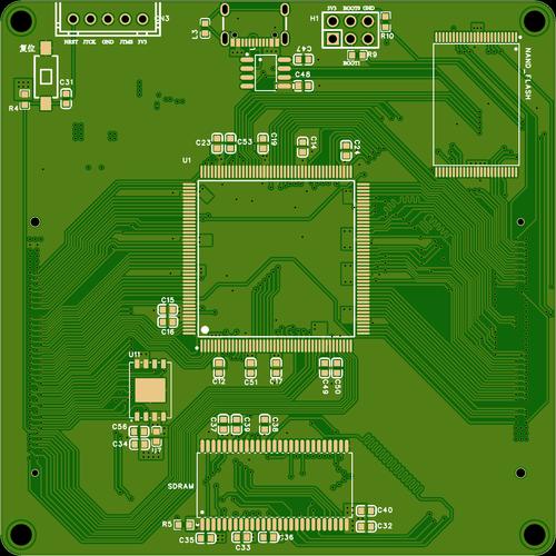
Screen printing, also known as silkscreen printing, is a fundamental process in printed circuit board (PCB) manufacturing that applies identifying markings, symbols, and labels onto the board surface. This critical step occurs after solder mask application but before surface finish and component assembly, serving as the primary visual guide for PCB assembly, testing, and maintenance. The screen-printed layer contains essential information such as component designators (R1, C2, U3), polarity indicators, company logos, and safety symbols that enable technicians to correctly place components and troubleshoot issues throughout the product lifecycle .
The importance of screen printing in modern electronics manufacturing cannot be overstated. As electronic devices evolve toward higher density and miniaturization, with component pitches shrinking below 0.3mm, the precision and clarity of screen-printed markings become increasingly critical for assembly accuracy. Industry data indicates that properly applied screen printing can reduce assembly errors by up to 40% and improve troubleshooting efficiency by 60%, making it a vital quality control element in PCB production. Furthermore, regulatory requirements mandate specific markings for compliance certifications (CE, UL, RoHS), making screen printing an essential aspect of product safety and market acceptance .
1. What is Screen Printing in PCB?
Screen printing in PCB manufacturing is a precision printing technique that transfers ink through a patterned mesh screen onto a circuit board’s surface to create functional markings and identifiers. This process utilizes a stencil-like screen containing open areas that correspond to the desired pattern, through which specialized ink is forced using a squeegee. The resulting markings typically include component reference designators, polarity indicators, test points, version information, and manufacturer logos, all of which serve critical functions in the PCB assembly and maintenance processes .
The technological foundation of PCB screen printing lies in the precise control of ink transfer through a mesh screen, which is typically constructed from polyester, nylon, or stainless steel with thread counts ranging from 120 to 400 threads per inch. Higher mesh counts enable finer details, with modern screens capable of achieving line widths as fine as 50-75μm (2-3 mils) for high-density applications. The screens are prepared by coating them with a light-sensitive emulsion, which is then exposed to UV light through a film positive of the circuit pattern. After development, the unexposed emulsion washes away, creating open areas that allow ink passage during printing .
From a materials perspective, screen printing employs specialized inks formulated for adhesion, durability, and legibility. Epoxy-based inks are most common, offering excellent resistance to heat (withstanding 288°C for 10 seconds during soldering), chemicals (flux, cleaning solvents), and mechanical abrasion. These inks typically exhibit viscosity in the range of 3,000-10,000 centipoise and must maintain consistent rheological properties throughout the printing process. For applications requiring enhanced environmental compatibility, UV-curable and water-based ink formulations have been developed, reducing volatile organic compound (VOC) emissions while maintaining performance characteristics .
2. PCB Screen Printing Symbols and Other Elements
PCB screen printing incorporates a standardized system of symbols and alphanumeric identifiers that provide essential information for assembly, testing, and maintenance. The most fundamental elements are reference designators, which follow the IEEE 315 standard for component identification: “R” for resistors, “C” for capacitors, “U” for integrated circuits, “D” for diodes, “L” for inductors, and “Q” for transistors, each followed by a numerical value indicating their position in the circuit schematic. These designators enable cross-referencing between the physical board, schematics, and bill of materials (BOM), ensuring correct component placement and facilitating troubleshooting activities .
Polarity and orientation indicators constitute another critical symbol category. Diodes are marked with a cathode band symbol, electrolytic capacitors display “+” indicators for positive terminals, and integrated circuits feature dots, notches, or tapered markings to identify pin 1 positions. Connectors typically include numerical designations starting from pin 1, often with directional arrows indicating mating orientation. These markings are particularly crucial for automated assembly processes, where optical recognition systems rely on clear, high-contrast patterns for component orientation verification. Studies indicate that proper polarity marking can reduce installation errors by up to 35% in high-volume production environments .
Table: Standard PCB Screen Printing Symbols and Specifications
| Symbol Type | Standard Representation | Minimum Size Guidelines | Placement Requirements |
|---|---|---|---|
| Reference Designators | R1, C5, U3 | Height: 0.8-1.2mm, Stroke: 0.15-0.2mm | 0.5mm from component outlines |
| Polarity Indicators | +, – symbols | Height: 0.6-1.0mm | Adjacent to relevant pads |
| Pin 1 Identifiers | Dot, notch, triangle | Diameter: 0.5-0.8mm | Clear association with pin 1 |
| Test Points | TP1, TP2 with circle | Height: 0.6-0.8mm | Unobstructed access |
| Warning Symbols | Exclamation marks in triangles | Height: 1.0-1.5mm | Near hazardous areas |
| Compliance Marks | CE, UL, RoHS logos | Height: 1.2-2.0mm | Board periphery |
Beyond component-level markings, PCB screen printing includes board-level information such as product identification numbers, revision codes, date stamps, serial numbers, and manufacturer logos. These elements support traceability throughout the product lifecycle, enabling recall management, warranty validation, and field service operations. Safety markings include electrostatic discharge (ESB) symbols near sensitive components, high-voltage warnings adjacent to dangerous circuits, and thermal cautions for heat-generating areas. Regulatory compliance marks (CE, FCC, UL) must meet specific size and clarity requirements dictated by the corresponding standards organizations, typically requiring minimum heights of 1.2mm for adequate legibility .
Design guidelines for PCB screen printing emphasize clarity, consistency, and contrast. The IPC-2615 standard recommends sans-serif fonts with width-to-height ratios between 1:5 and 1:10 for optimal readability. Text should be oriented uniformly (0° or 90° rotation) to facilitate quick scanning, and important markings should maintain a minimum distance of 0.25mm from solderable pads to prevent ink contamination. For high-density boards with limited space, abbreviated markings and strategic positioning under components may be employed, though these require careful planning to maintain functionality without compromising manufacturability .
3. How is PCB Screen Printing Done? Screen Printing Methods
The PCB screen printing process begins with comprehensive pre-production preparation, starting with the transformation of design data into a printable stencil. CAD files containing the silkscreen layer are imported into specialized software that generates high-resolution film positives, typically with a resolution of 5,000-8,000 dpi to ensure edge definition. Meanwhile, the screen mesh is selected based on the required printing precision—standard applications use 160-230 threads per inch meshes, while high-density designs may require 305-355 threads per inch for finer details. The mesh is tensioned to 20-25 N/cm² on aluminum frames to ensure dimensional stability during printing .
The actual printing process involves precise synchronization of multiple parameters. The prepared screen is mounted in the printer and aligned with the PCB using optical registration systems achieving ±25μm accuracy. Ink is deposited on one end of the screen, and a polyurethane squeegee with a hardness of 60-80 Shore moves across the surface at 10-30 cm/sec with 0.3-0.5 MPa pressure, forcing ink through the mesh openings onto the board. The squeegee angle is critical—maintained at 60-75°—to ensure complete mesh contact without excessive deformation. The snap-off distance (gap between screen and PCB) is typically set at 0.5-1.0mm to allow clean separation after ink deposition .
Table: Comparison of PCB Screen Printing Methods
| Method | Resolution Capability | Production Speed | Cost Factors | Ideal Applications |
|---|---|---|---|---|
| Manual Screen Printing | 100-150μm | 10-20 boards/hour | Low equipment cost, high labor | Prototypes, small batches |
| Semi-Automatic Printing | 75-100μm | 30-50 boards/hour | Moderate investment | Medium-volume production |
| Full-Automatic Printing | 50-75μm | 100-300 boards/hour | High equipment cost | High-volume manufacturing |
| Direct Legend Printing (DLP) | 30-50μm | 20-40 boards/hour | Moderate equipment cost | Quick-turn, high-mix |
Post-printing processes focus on ink stabilization and quality verification. The printed boards undergo curing through thermal or UV methods—thermal curing typically involves 15-30 minutes at 120-150°C to cross-link epoxy resins, while UV curing utilizes 300-400 mJ/cm² exposure for near-instantaneous hardening. Quality inspection employs automated optical inspection (AOI) systems comparing printed patterns against reference designs with 10-20μm accuracy, flagging defects like smearing, bridging, or misregistration. Additional tests include adhesion assessment via tape peel tests, chemical resistance verification through flux exposure, and thermal stability evaluation by subjecting samples to multiple solder reflow cycles .
Advanced printing methodologies have emerged to address specific manufacturing challenges. Direct Legend Printing (DLP) uses inkjet technology to deposit acrylic inks directly from digital files, eliminating screen preparation time and enabling real-time content modifications. Liquid Photo Imaging (LPI) applies a photosensitive epoxy layer across the entire board, which is then exposed to UV light through a photomask, developing high-resolution patterns down to 30μm line widths. These methods offer distinct advantages for high-mix production environments where flexibility and rapid turnaround are prioritized over maximum throughput .
4. PCB Screen Printing Guidelines
Effective PCB screen printing requires adherence to established design guidelines that balance readability with manufacturing constraints. Text size specifications must consider both legibility and available space—primary component designators should maintain a minimum height of 0.8mm with stroke widths of 0.15mm, while secondary information can be reduced to 0.6mm height in dense layouts. For miniature components like 0201 packages or fine-pitch BGAs, reduced marking sizes may be necessary, but should never fall below 0.5mm height even in the most constrained scenarios. The aspect ratio of text (height to width ratio) should remain between 1:5 and 1:10 to ensure character recognition across various viewing angles .
Placement rules govern the spatial relationship between screen printing and other PCB elements. Critical markings must maintain a 0.3mm clearance from solderable pads to prevent ink contamination that could compromise solder joint formation. Component outlines should extend beyond the actual component footprint by 0.2-0.5mm to provide visual guidance during placement without interfering with the component body. Polarity indicators should be positioned adjacent to the corresponding pad with unambiguous orientation—for example, “+” symbols should be placed within 0.5mm of positive terminals with consistent alignment relative to the component center. Reference designators should be located near the component but not underneath it, ensuring visibility after assembly .
Material selection guidelines address the compatibility between inks and PCB substrates. Standard FR-4 boards typically use epoxy-based inks cured at 120-150°C, while flexible polyimide circuits require modified epoxy or polyurethane formulations with lower curing temperatures (80-120°C) to prevent substrate damage. For high-temperature applications such as automotive under-hood components or aerospace systems, ceramic-filled inks capable of withstanding 200-300°C continuous operation are essential. Special surface finishes like immersion silver or ENIG require inks with specific adhesion promoters, whereas HASL surfaces can accommodate standard formulations. The ink color should provide sufficient contrast with the solder mask—white on green offers the highest readability, while yellow on green may require larger text sizes for equivalent legibility .
Process control parameters must be optimized for consistent results. Ink viscosity should be maintained within ±5% of the target value (typically 3,000-8,000 cP) through temperature control and regular stirring. The printing environment should be maintained at 23±3°C and 40-60% relative humidity to prevent viscosity fluctuations and ensure proper curing characteristics. Squeegee durometer, angle, and pressure should be calibrated based on mesh count—higher mesh counts require softer squeegees (60-70 Shore) and lower pressures (0.2-0.3 MPa) to prevent mesh damage while ensuring complete ink transfer. Regular maintenance schedules should include screen tension checks (maintained above 20 N/cm²), squeegee edge inspection, and stencil cleaning to prevent defect accumulation .
5. What Can Damage the Screen Printing Layer on PCB?
The screen printing layer on PCBs is susceptible to various forms of damage throughout the manufacturing and product lifecycle, with mechanical abrasion representing a primary failure mechanism. During assembly, handling procedures can cause scratches or partial removal of ink, particularly when boards are stacked without protective separators or when abrasive materials contact the surface. Automated component insertion equipment may generate friction that wears away markings, especially if ink adhesion is compromised or curing parameters are suboptimal. Testing procedures involving probe cards or bed-of-nails fixtures exert localized pressure that can fracture ink, particularly near test points where repeated contact occurs. Studies indicate that improperly cured inks can experience up to 40% greater wear rates compared to fully cured counterparts when subjected to mechanical stress .
Chemical exposure presents another significant threat to screen printing integrity. Flux residues from soldering processes, particularly no-clean formulations with acidic activators, can penetrate partially cured inks and initiate degradation through swelling or embrittlement. Cleaning solvents—especially those containing ketones or glycol ethers—may dissolve ink binders if the ink formulation lacks specific chemical resistance. Environmental contaminants like plasticizers outgassing from wire insulation or sulfur compounds present in industrial atmospheres can cause ink discoloration and loss of adhesion over extended periods. Accelerated testing reveals that inks with inadequate chemical resistance may show visible degradation after 100-200 hours exposure to typical flux environments, whereas compliant formulations maintain integrity beyond 1,000 hours .
Thermal stress factors include both process-induced and operational temperature exposures. During PCB fabrication, multiple solder reflow cycles subject screen printing to peak temperatures of 240-260°C for lead-free processes, potentially causing cracking or delamination if the ink’s coefficient of thermal expansion (CTE) mismatches the substrate. In service, power cycling generates repeated thermal expansion that mechanically stresses the ink-board interface, leading to progressive failure. Ultraviolet radiation from sunlight or artificial lighting can photochemically degrade ink pigments and binders, resulting in fading that reduces contrast and legibility. Thermal cycling tests demonstrate that quality screen printing should withstand at least 100 cycles between -40°C and +125°C without significant degradation, meeting the requirements of most commercial and industrial applications .
Table: Screen Printing Failure Modes and Prevention Strategies
| Damage Type | Primary Causes | Prevention Methods | Testing Standards |
|---|---|---|---|
| Mechanical Abrasion | Handling, testing, installation | Proper curing, protective coatings | IPC-SM-840 abrasion test |
| Chemical Degradation | Flux, solvents, contaminants | Chemical-resistant ink formulations | IPC-TM-650 solvent resistance |
| Thermal Damage | Reflow soldering, power cycling | CTE-matched inks, thermal stabilizers | JEDEC JESD22-A104 thermal cycling |
| UV Fading | Sunlight, artificial lighting | UV-stable pigments, protective coatings | ASTM G154 QUV testing |
| Adhesion Failure | Surface contamination, poor curing | Surface preparation, adhesion promoters | ASTM D3359 cross-cut test |
Manufacturing process errors constitute a preventable category of screen printing damage. Incomplete curing—resulting from insufficient time, temperature, or UV exposure—leaves inks vulnerable to subsequent processing steps. Contamination of the PCB surface prior to printing, including oils from handling or dust particles, creates weak adhesion points where ink can detach. Registration errors causing misalignment may not immediately damage the ink, but necessitate removal processes that can harm both the marking and underlying solder mask. Statistical process control data indicates that 70% of screen printing defects originate from preparation and process parameter issues rather than material deficiencies, highlighting the importance of procedural discipline .
Environmental factors specific to the product’s operating environment can progressively degrade screen printing. High-humidity conditions promote hydrolysis of ink binders, particularly in polyester-based formulations, leading to blistering or peeling. Ozone exposure in polluted urban environments or industrial settings causes oxidation that embrittles ink polymers. Microbial growth in tropical climates can physically disrupt markings and secrete enzymes that degrade organic components of ink formulations. For extreme environments, specialized ink systems with enhanced resistance profiles are available, though at increased cost—typically 20-30% premium over standard formulations, justified by demonstrated lifespan extensions of 3-5 times in aggressive conditions .
6. Screen Printing PCB Repair and Rework
Screen printing repair procedures vary based on the extent and nature of damage, with localized repair techniques addressing minor defects. For isolated marking omissions or errors, precision dispensing systems equipped with micro-nozzles (**
100-200μm diameter) can apply touch-up ink matching the original formulation. The repair area must first be cleaned with isopropyl alcohol and lightly abraded using fine bristle brushes or erasers to improve adhesion. After ink application, localized curing employs miniature heat nozzles or UV LEDs that deliver energy precisely to the repair site without affecting surrounding components. For the most critical applications, laser marking systems can directly engrave markings into the solder mask, creating permanent identifiers without additional materials. These micro-repair techniques typically restore 90-95%** of the original legibility when performed by skilled technicians .
Complete screen printing rework becomes necessary when widespread defects or functional requirements mandate full layer replacement. The removal process begins with chemical softening using specialized strippers that penetrate the ink layer without damaging underlying solder mask. Mechanical removal employs non-abrasive plastic scrapers and nylon brushes under controlled pressure to lift ink without scoring the substrate. For stubborn deposits, laser ablation systems can selectively remove ink through precise thermal degradation, though this requires careful power calibration to prevent solder mask damage. Post-removal cleaning involves sequential washes with neutral pH cleaners and deionized water, followed by surface activation through plasma treatment or chemical etching to ensure optimal adhesion for the new printing layer .
Table: Screen Printing Repair Methods and Applications
| Repair Method | Equipment Requirements | Typical Repair Time | Success Rate | Limitations |
|---|---|---|---|---|
| Manual Touch-up | Micro-dispenser, magnifier | 5-15 minutes per marking | 85-90% | Requires skilled operator |
| Stencil Patch | Partial stencil, alignment jig | 10-20 minutes per area | 92-95% | Limited to accessible areas |
| Laser Engraving | Fiber laser system | 2-5 minutes per marking | 98%+ | Permanent alteration |
| Inkjet Patch | Precision inkjet head | 3-8 minutes per marking | 90-93% | Color matching challenges |
Post-repair validation ensures that repaired screen printing meets original specifications. Adhesion testing follows IPC-TM-650 methods using pressure-sensitive tape applied perpendicular to the surface and rapidly removed—acceptable repairs show no ink transfer to the tape. Legibility assessment employs optical character verification systems comparing repaired markings to reference fonts with 95% similarity threshold requirements. Thermal stability verification subjects samples to simulated reflow profiles, requiring survival of three cycles at peak temperatures of 260°C without cracking, lifting, or discoloration. Chemical resistance testing involves exposure to flux, isopropyl alcohol, and common cleaning solvents for 60 seconds with no visible degradation .
Advanced repair methodologies incorporate digital restoration techniques where damaged or missing markings are recreated from original design data. High-resolution scanners capture the existing printing pattern, which software then compares to the reference design, highlighting discrepancies for prioritized repair. For boards with damaged solder mask beneath the screen printing, combined repair processes must first restore the mask layer using epoxy patching compounds cured at moderate temperatures (80-100°C), followed by screen printing application once the patch is fully hardened. The most challenging repairs involve multi-layer markings where different information overlaps—these require sequential removal and recreation using registration systems maintaining ±25μm alignment accuracy to preserve original appearance and function .
Conclusion
Screen printing remains an indispensable technology in PCB manufacturing, providing critical visual guidance for assembly, testing, and maintenance throughout the product lifecycle. Despite the emergence of alternative marking technologies, screen printing’s unique combination of cost-effectiveness, durability, and versatility ensures its continued relevance across electronics industries. The process has evolved significantly from its manual origins to incorporate advanced automation, precision materials, and sophisticated quality control methods that meet the demanding requirements of modern high-density PCB designs .
The future of PCB screen printing will likely focus on addressing the challenges posed by ongoing miniaturization trends while enhancing environmental sustainability. Digital printing technologies like Direct Legend Printing (DLP) offer promising alternatives for high-mix, quick-turn production environments, though traditional screen printing will maintain dominance in high-volume applications. Material developments will focus on eco-friendly formulations with reduced VOC content and improved recyclability, without compromising the thermal and chemical resistance required for lead-free soldering processes. As electronics continue to proliferate across industries, the humble screen-printed marking will remain an essential contributor to manufacturing efficiency and product reliability .


0 Comments