
Introduction
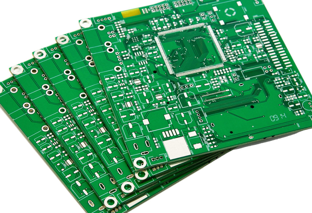
A PCB module is a core component in modern electronic devices, referring to an independent circuit unit on a printed circuit board (PCB) that performs a specific function through standardized design. Against the backdrop of increasingly complex electronic equipment, the modular design of PCBs has become a significant trend in the electronics industry. This design approach breaks down complex circuit systems into functionally independent modules—such as power supply modules, communication modules, and data processing modules—greatly enhancing the maintainability and upgrade efficiency of electronic devices .
As the global electronics industry moves toward higher density and greater reliability, the importance of PCB modular design has become even more prominent. It not only simplifies the design and manufacturing processes of electronic products but also enables optimization and innovation of different circuit units through the standardization of functional units. From smartphones to automotive electronics, and from industrial controls to medical devices, PCB modular technology is reshaping the design philosophy and manufacturing methods of electronic products, bringing unprecedented flexibility and reliability to the electronics industry .
1. What is a PCB Module
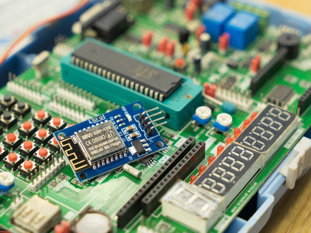
A PCB module is a functional unit circuit based on printed circuit board technology. It integrates electronic components and traces for a specific function into a standalone hardware unit that can operate independently or in coordination with other modules. Structurally, a PCB module typically includes a substrate, conductive traces, electronic components, and interfaces. Through standardized packaging and interface definitions, it achieves specific functions. Compared to ordinary PCBs, PCB modules place greater emphasis on functional completeness and interface standardization, allowing them to be designed, tested, and replaced as independent units .
The basic composition of a PCB module includes four main parts: the substrate material, conductive layers, components, and interfaces. The substrate is usually made of FR-4 epoxy glass cloth, metal base, or flexible materials, chosen according to application requirements. The conductive layer is formed by patterning copper foil to create circuit connections, with the number of layers ranging from single to multi-layer. Components include integrated circuits, resistors, capacitors, inductors, and other active and passive elements, installed via surface mount technology (SMT) or through-hole technology (THT). The interface section ensures electrical connection and mechanical fixation between the module and the external system, such as board-to-board connectors or pins .
From a design perspective, the fundamental difference between PCB modules and traditional PCBs lies in the modular design philosophy. Traditional PCB design emphasizes the integrity of the overall circuit, with all circuit functions implemented on a single board. In contrast, modular PCB design breaks down complex systems into multiple, relatively independent functional sub-modules that communicate and collaborate through standardized interfaces. This design approach makes electronic systems more flexible, easier to maintain and upgrade, and significantly improves design efficiency and quality reliability .
2. Design Principles and Core Elements of PCB Modules
The design of a PCB module is a systematic project that requires comprehensive consideration of multiple factors, including electrical performance, thermal management, and signal integrity. First, reasonable layout planning is the foundation. Partition layout should be carried out according to signal flow and interference levels. Various circuit modules should be divided based on function, frequency, and signal type to ensure the rationality of the overall layout, achieving short overall routing paths and no interference between modules. For example, in laboratory analytical instruments, the typical signal flow is “sampling → preprocessing → separation → detection → data processing.” Modules should be arranged linearly in this sequence, with the distance between modules usually controlled within 10cm to reduce signal transmission delay .
The layout of special components is crucial to module performance. The clock circuit, as the largest source of interference on a board, should be kept away from board edges and unrelated circuits, and the trace from the clock output to the load should be as short as possible. The power supply section should be placed near the board’s power entry point, and the power section should be isolated from other circuit parts using via strips or split lines. Electromagnetically sensitive components like inductor coils should be kept away from noise sources such as switching power supplies and clock outputs, and no high-speed or sensitive control lines should be routed underneath the coil on the PCB .
Table: Classification Principles of PCB Module Layout
| Classification Method | Module Type | Layout Requirements | Typical Application |
|---|---|---|---|
| By Function | Power supply module, signal processing module, interface module | Arranged according to signal flow to avoid crossover | Industrial control systems |
| By Frequency | High-frequency circuit, intermediate-frequency circuit, low-frequency circuit | Arranged in order of high, medium, low without overlap | RF communication equipment |
| By Signal Type | Digital circuit, analog circuit | Partitioned layout, with data conversion circuits at the junction | Data acquisition systems |
Routing design is key to ensuring signal integrity. High-speed signal lines should preferably be routed on inner layers and undergo necessary matching and shielding. The length of control signal traces should be ≤10cm, the trace width should be ≥0.3mm, and the spacing from power signal traces should be ≥5mm. For high-speed data interfaces (such as PCIe), differential signal transmission should be used. The differential pair impedance needs to be controlled within 90Ω±10%, and the length difference should be ≤0.5mm. The width of power traces should be determined based on the current magnitude; generally, a 1mm wide trace can carry 1A of current. Traces for larger currents need to be widened accordingly .
Thermal management is an important part of module design. For high-power modules, thick copper boards (copper thickness ≥2oz) should be used to improve current carrying capacity and heat dissipation efficiency. Heat should be evenly distributed across the PCB through large-area ground planes and thermal via designs. In extreme environments, liquid cooling technology can be combined to ensure stable operation of power modules in environments up to 125°C .
3. Core Functions and Performance Parameters of PCB Modules
The core functions of PCB modules are mainly reflected in four aspects: electrical connection, signal transmission, power distribution, and system protection. The electrical connection function is the foundation, achieving reliable connections between components through wires, pads, and vias on the PCB. The signal transmission function requires the module to ensure the integrity of various signals (especially high-speed signals), including control signals, data signals, and status signals. The power distribution function involves efficiently delivering electrical energy to each functional unit, requiring consideration of parameters such as current capacity, voltage drop, and efficiency. The system protection function includes circuits for overcurrent, overvoltage, overtemperature, etc., ensuring the reliability of the module under various operating conditions .
The key performance parameters of PCB modules can be divided into three categories: electrical performance, thermal performance, and mechanical performance. Electrical performance parameters include operating voltage (e.g., 3.3V, 5V, 12V, etc.), current capacity (up to several hundred amperes), impedance control (e.g., single-ended 50Ω, differential 100Ω), signal rate (up to 25Gbps or higher), etc. Thermal performance parameters include maximum operating temperature (commercial grade 0-70°C, industrial grade -40 to 85°C, automotive grade -40 to 125°C) and thermal resistance coefficient (°C/W). Mechanical performance parameters include dimensional tolerance (usually ±0.1mm), board thickness (commonly 0.4-3.2mm), and bending strength, among others .
Table: Comparison of Key Performance Parameters of Different Types of PCB Modules
| Module Type | Typical Layers | Line Width/Spacing | Impedance Control | Special Processes |
|---|---|---|---|---|
| Communication Equipment Module | 16-30 layers | 3-4mil | ±5% | Back drilling, blind/buried vias |
| Automotive Electronics Module | 8-12 layers | 4-5mil | ±10% | Thick copper, high Tg materials |
| Consumer Electronics Module | 6-8 layers | 2-3mil | ±7% | HDI, laser microvias |
| Industrial Control Module | 4-8 layers | 5-6mil | ±10% | Thick copper, high voltage resistance |
Taking automotive electronics modules as an example, their performance parameters must meet stringent automotive standards. For instance, an ADAS control module needs to operate stably within a temperature range of -40°C to 125°C, using an 8-12 layer board design combined with blind/buried via technology and high Tg (≥170°C) materials to ensure reliability under harsh environments such as vibration and shock. The voltage acquisition error of a Battery Management System (BMS) module needs to be <0.1%, supporting a line width accuracy of 0.05mm and passing high/low-temperature cycle tests from -40°C to 125°C .
High-frequency modules (such as 5G antenna modules) place particular emphasis on signal integrity performance, requiring strict impedance control (±5%), the use of high-frequency low-loss materials (such as Megtron6, RO4350B), and back-drilling technology to improve signal purity. Power modules (such as vehicle power supplies), on the other hand, focus on electrical performance. Thick copper boards (4-6oz) can increase current carrying capacity by 30%, and conversion efficiency can reach over 96% .
4. Analysis of the Main Advantages of PCB Modules
Modular PCB design offers significant advantages in multiple aspects. The primary advantage is a substantial improvement in maintenance efficiency. By decomposing complex circuit systems into functionally independent modules, when a device fails, technicians can quickly locate the faulty module and replace it directly, without the need to troubleshoot and repair the entire circuit board, reducing the Mean Time To Repair (MTTR) by more than 50%. This modular maintenance approach is particularly suitable for applications sensitive to downtime, such as industrial control and communication equipment .
The second major advantage is design flexibility and upgrade convenience. When upgrading equipment, simply replacing or adding the corresponding functional modules can achieve performance improvements or functional expansions. For example, replacing the data processing module in industrial control equipment with a higher-performance one can increase processing speed; adding a new communication module to a smart home system can enable compatibility with more smart devices. This flexibility significantly reduces the development cost and time for product iterations, supporting companies in responding quickly to market changes .
The third advantage is improved production efficiency. Modular design facilitates parallel production, where different specialized teams can be responsible for the development and manufacturing of different modules simultaneously, significantly shortening the product time-to-market. Standardized modules also make it easier to achieve automated production, improving product consistency and quality reliability while reducing production costs. Studies show that modular design can reduce production costs by 20%-30%, making it particularly suitable for products requiring large-scale manufacturing .
The fourth advantage is enhanced reliability. PCB modular design allows for independent and sufficient testing and verification of each module, ensuring the performance and quality of each subsystem is optimized. For instance, in the automotive electronics sector, PCB modules for powertrain systems need to pass automotive-grade certifications like AEC-Q100 to ensure high reliability in harsh environments. Meanwhile, modular design reduces the complexity of the overall system, minimizing the impact of single points of failure on the system .
Finally, PCB modularization benefits technology reuse and standardization. Mature functional modules can be reused in different products, reducing redundant development and improving design efficiency. The definition of industry-standard module interfaces promotes supply chain standardization, allowing companies to procure compatible modules from multiple suppliers, reducing procurement risks and costs. This technology reuse significantly increases the return on investment in R&D resources and accelerates the development speed of new products .
5. Main Types and Application Fields of PCB Modules
PCB modules can be classified into various types based on their function, structure, and application scenario. Classified by function, they mainly include power supply modules, signal processing modules, communication modules, control modules, and sensor modules. Power supply modules are responsible for power conversion and distribution, such as DC-DC converter modules. Signal processing modules contain various analog and digital signal processing circuits. Communication modules enable wired and wireless communication functions. Control modules act as the system core to execute control algorithms. Sensor modules are responsible for collecting environmental parameters .
Classified by structural characteristics, PCB modules include rigid modules, flexible modules, and rigid-flex modules. Rigid modules use rigid substrates and are suitable for most general scenarios. Flexible modules use bendable materials and are suitable for space-constrained or movable devices. Rigid-flex modules combine the advantages of both and are important in high-end fields such as aerospace and medical equipment. Classified by layer structure, there are single-sided modules, double-sided modules, and multi-layer modules. The more layers, the higher the wiring density and design flexibility .
Table: Application Characteristics of PCB Modules in Different Industries
| Application Field | Typical Module Types | Technical Requirements | Representative Products |
|---|---|---|---|
| Communication Equipment | 5G antenna module, base station main control board | High frequency, precise impedance, multi-layer high-speed signal lines | 5G base station equipment |
| Automotive Electronics | ADAS control unit, BMS module | High reliability, vibration resistance, high Tg materials | New energy vehicle control system |
| Industrial Control | PLC control board, motor drive board | High voltage resistance, thick copper design, anti-interference | Industrial automation system |
| Medical Equipment | CT scanning system, ECG analysis module | High precision, high density, signal integrity | Medical diagnostic equipment |
| Consumer Electronics | Mobile phone motherboard, camera module | HDI structure, blind/buried vias, miniaturization | Smartphones, tablets |
In the field of communication equipment, PCB modules require high frequency and high performance. For example, antenna modules in 5G base stations use 16-30 layer multi-layer board designs, require strict impedance control (±5%), use high-frequency low-loss materials (e.g., Megtron6), and apply back-drilling and blind/buried via technologies to enhance signal integrity. These modules need to support high-speed signal transmission (above 25Gbps) while meeting the temperature and humidity requirements of outdoor environments .
Automotive electronics is one of the fastest-growing application areas for PCB modules. With the popularity of new energy vehicles, in-vehicle power supplies, Battery Management Systems (BMS), and fast-charging modules place higher demands on PCB modules. For instance, ADAS control modules use 8-12 layer board designs combined with thick copper technology (≥2oz) and high Tg materials (≥170°C) to ensure reliability within the temperature range of -40°C to 125°C. BMS modules require precise voltage acquisition (error <0.1%) and good thermal management capabilities .
PCB modules in the industrial control field emphasize reliability and durability. PLC control boards and motor drive modules need to use thick copper designs (2-6oz) to improve current carrying capacity and pressure resistance, ensuring long-term stable operation in harsh industrial environments. These modules typically need to comply with IP protection ratings, resist electromagnetic interference, and support industrial bus communication protocols .
Medical electronics have extremely high requirements for the precision and reliability of PCB modules. PCB modules in medical equipment such as CT scanning systems and ECG analysis modules require high-density wiring, fine lines (line width/spacing ≤3mil), and ensure the accuracy of signal acquisition and transmission. Additionally, these modules need to meet biocompatibility requirements, especially in implantable medical devices .
6. Frequently Asked Questions About PCB Modules
What is the main difference between a PCB module and an ordinary PCB board?
The main difference between a PCB module and an ordinary PCB board lies in the design philosophy and functional integrity. An ordinary PCB board typically serves as a carrier for the overall circuit, with all functional circuits designed on the same board. In contrast, a PCB module emphasizes functional independence and interface standardization. Each module performs a specific function and works collaboratively with other modules through standard interfaces. This modular design makes the system more flexible and easier to maintain and upgrade. For example, in laboratory analytical instruments, different functional modules (such as solvent delivery modules, injection modules, detection modules) can be laid out independently according to the signal flow and interconnected through standardized interfaces, reducing mutual interference and facilitating fault diagnosis and module replacement .
How to evaluate the quality and reliability of a PCB module?
Evaluating the quality and reliability of a PCB module requires consideration from multiple dimensions. First is material selection, including parameters such as the substrate’s Tg value (glass transition temperature), coefficient of thermal expansion (CTE), and heat resistance. Automotive electronics modules typically require Tg ≥170°C and excellent high-temperature performance. Second is the process level, such as line width accuracy, pad alignment, and hole wall quality. Third is environmental adaptability, verified through tests like temperature cycling (e.g., -40°C to 125°C), vibration testing, and damp heat testing. Furthermore, electrical performance parameters such as insulation resistance, dielectric withstand voltage, and signal integrity are also important indicators. Industry standard certifications (e.g., ISO9001, IATF16949, UL certification) can also serve as references for reliability assessment .
What are the advantages of applying High-Density Interconnect (HDI) technology in PCB modules?
The advantages of applying HDI technology in PCB modules are mainly reflected in three aspects: First, it increases wiring density, allowing for higher integration through microvias (<0.1mm) and fine lines (line width/spacing ≤3mil), meeting the miniaturization needs of portable devices. Second, it improves signal integrity by reducing the number of vias and optimizing signal paths, which is beneficial for high-speed signal transmission. Third, it enhances thermal management capabilities by improving thermal pathway design, thereby increasing the power density of the module. In consumer electronics modules like smartphone motherboards, HDI technology (using first/second order blind and buried vias) is a key technology for achieving high-density wiring, supporting extremely thin board designs of 0.4-0.6mm while ensuring high-precision impedance control .
How to solve the heat dissipation problem of high-power PCB modules?
Solving the heat dissipation problem of high-power PCB modules requires comprehensive measures. The primary step is selecting appropriate substrate materials, such as metal core boards (aluminum base, copper base) or highly thermally conductive insulating materials, to improve heat conduction efficiency. Secondly, increasing the copper thickness (2-10oz) expands the heat conduction cross-section, supporting high current passage while reducing temperature rise. Third, optimize the layout design, placing high-power devices in positions with good heat dissipation and in direct contact with heat dissipation devices. Fourth, use thermal vias to enhance interlayer heat transfer. Additionally, external heat dissipation solutions such as heat sinks, fans, or liquid cooling systems can be combined to achieve “passive + active” dual heat dissipation. For example, in fast-charging modules, combining a 6oz thick copper board with a micro fan can reduce the peak temperature from 110°C to 75°C, significantly extending the module’s lifespan .
7. Development Prospects and Trends of PCB Modules
PCB module technology is rapidly developing towards three major directions: high performance, integration, and green manufacturing. In terms of high performance, with the popularization of 5G communication, artificial intelligence, and IoT technologies, the demand for high-speed, high-frequency PCB modules is growing. Data shows that the number of layers in server motherboard modules has developed from the ordinary 8-12 layers to 24-32 layers, supporting higher speed signal transmission (56Gbps and above). Meanwhile, material technology is also constantly innovating. The application of wide-bandgap semiconductor materials such as Gallium Nitride (GaN) and Silicon Carbide (SiC) significantly increases the operating frequency and efficiency of power modules .
Integration is another important trend. Through System-in-Package (SiP) and embedded component technology, multiple chips and components are integrated into a single module, further increasing functional density. For example, the power module developed based on GaN PCB embedded packaging reduces the volume of the main drive motor controller for hybrid electric vehicles by 30%, costs by more than 15%, and improves the average efficiency under WLTC conditions by 2%. This integrated module is particularly suitable for application scenarios with limited space, such as automotive electronics and portable devices .
Green manufacturing has become an unavoidable development direction for the PCB module industry. With increasingly stringent environmental regulations, the PCB manufacturing industry is actively adopting environmentally friendly materials such as lead-free solder and halogen-free flame retardants, and optimizing production processes to reduce wastewater and exhaust gas emissions. For example, the application of micro-etchant regeneration technology enables the treatment and recycling of waste liquid during the etching process, significantly reducing environmental pollution. In the future, biodegradable substrate materials and low-energy manufacturing processes will further promote the sustainable development of PCB modules .
From the perspective of application fields, new energy vehicles, medical electronics, and aerospace will be important growth areas for PCB module technology. In the field of new energy vehicles, with the popularization of 800V high-voltage platforms and ultra-fast charging technology, thick copper board technology (up to 12oz) will continue to innovate to meet high power density requirements. In the field of medical electronics, the development of biocompatible PCB modules will promote innovative products such as swallowable sensors and degradable electronic devices. The expansion of these application fields will bring new challenges and opportunities for PCB module technology .
Future development trends of PCB module technology also include:
- Higher density interconnection technology, such as mSAP (modified Semi-Additive Process) supporting finer lines (below 15µm).
- Application of higher frequency materials, supporting high-frequency applications like 77GHz automotive radar and terahertz communication.
- Embedded component technology, embedding passive components into the board to improve surface area utilization.
- AI-assisted design, using AI algorithms to optimize module layout and routing, improving design efficiency .
Summary
As the cornerstone of modern electronic equipment, PCB modules efficiently organize and manage complex electronic systems through a modular design philosophy. From basic concepts to design principles, and from core functions to application scenarios, PCB module technology has formed a complete system and plays an irreplaceable role in fields such as communications, automotive, industrial, and medical applications. As electronic equipment develops towards higher performance, smaller size, and lower power consumption, PCB module technology will continue to innovate, providing more advanced solutions for the electronics industry .
In the future, with the introduction of new materials, new processes, and new design concepts, PCB modules will evolve towards higher integration, higher performance, and greater environmental friendliness. As the “invisible pillar” of electronic products, PCB module technology will continuously break through existing limitations, assisting the global electronics industry towards a smarter, more efficient, and sustainable future .


0 Comments