
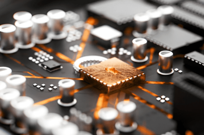
Have you ever opened up any electronic device, whether it’s a mobile phone, computer, or television, and seen a board covered with lines and components? That board is a Printed Circuit Board (PCB), the cornerstone of modern electronic devices. Just like a city’s road system, it connects all electronic components together, enabling them to work in harmony.
What is a PCB?
PCB stands for Printed Circuit Board. It is a board processed to a certain size from an insulating substrate as the base material, featuring at least one conductive pattern and all designed holes on it to achieve electrical interconnection between components.
Simply put, a PCB is a carrier that uses copper etching technology to form predetermined circuit patterns on an insulating substrate, allowing electronic components to be connected according to the design.
When a standard PCB has no components on it, it is also referred to as a “Printed Wiring Board” (PWB). PCBs are found in almost every type of electronic device, from small electronic watches and calculators to large computers, communication electronics, and military weapon systems. Whenever there are integrated circuits or other electronic components, PCBs are used for their electrical interconnections.
The Structure of a PCB
The structure of a PCB is a complex integration of numerous parts. Each element plays its own role in the manufacturing and operation of the PCB. The manufacturing and assembly of PCBs strictly follow standard processes. Understanding how a PCB works aids in better design and troubleshooting. Although a PCB contains many parts, they can be broadly categorized into the following types:
- Substrate
The core part of the PCB is called the substrate. It provides structural stability to the PCB and isolates the layers, components, and copper traces. The substrate layer is typically a rigid board made of glass fiber-reinforced epoxy material. For flexible PCBs, polyimide materials are used to give the board suitable flexibility, which is crucial for the proper functioning of PCBs in flexible electronics. - Copper Layer
A thin layer of copper is deposited on the substrate layer. Because copper is a good conductor of electricity, it is a cost-effective solution in PCB manufacturing. Depending on the type of PCB, the copper layer can be applied to one side (single-sided) or both sides (double-sided) of the PCB. In multi-layer stack-ups, the required number of copper layers are stacked, with insulating material sandwiched between each two copper layers. The trace layout does not require the entire copper plane; therefore, the unneeded parts are etched away. The width, length, and height of the traces must be precisely controlled, as does the etching of the desired copper traces. This is the key step enabling current flow and signal transmission in the PCB. - Solder Mask
A protective coating is applied over the copper layer to prevent short circuits and copper oxidation. The solder mask also ensures that solder is only applied to designated areas on the PCB. The common green coating on the top of a PCB is the solder mask. It directly affects the proper functioning of the PCB by maintaining insulation and preventing short circuits. - Components
The core function of any PCB is to allow, process, limit, or store power or data signals, thereby generating the corresponding output. The PCB is equipped with various components to support these functions. Based on size and packaging, electronic components can be divided into PTH (Plated Through-Hole) and SMD (Surface Mount Device). Based on power response, components are categorized as active or passive. These components are soldered onto dedicated pads or holes on the conductive layer of the PCB. This interaction illustrates how the PCB works to achieve the desired performance. - Holes and Vias
Copper foil traces are used to connect the various components on the PCB. Precisely sized holes are drilled into the PCB for inserting PTH components. Typically, hole positions are marked at the ends of traces. Two holes on the same trace constitute a short circuit. In multi-layer stack-ups, blind vias or buried vias are set to connect the different layers. Power or signals are transmitted between layers through these vias. - Terminals and Connectors
The PCB board is equipped with input/output terminals and connectors. The PCB receives the required signals, processes them, and produces the output needed for the final application. To connect the PCB to other peripherals or accessories, connectors are also provided in the PCB assembly. In some PCB applications, additional jumpers and wires might also be used. - Silkscreen
A Printed Circuit Board (PCB) presents a complex circuit layout. To identify components and other information on the PCB, a silkscreen layer containing component identification symbols and markings is added to the board after the manufacturing process is complete. The silkscreen aids in understanding the circuit layout, thus facilitating assembly, troubleshooting, and repair work.
Classification and Diversity of PCBs
PCBs can be classified into various types based on different structures and materials, each with its specific application scenarios.
Classified by number of layers, PCBs can be single-sided, double-sided, or multi-layer boards.
- Single-Sided Boards are the simplest type of PCB. Components are concentrated on one side, and traces are on the other. Because traces are only on one side, there are many strict design limitations. They are often used in early circuits or simple products.
- Double-Sided Boards are an extension of single-sided boards. They are used when single-layer routing cannot meet the needs of the electronic product. Both sides have copper cladding and traces, and vias can be used to connect circuits between the two layers.
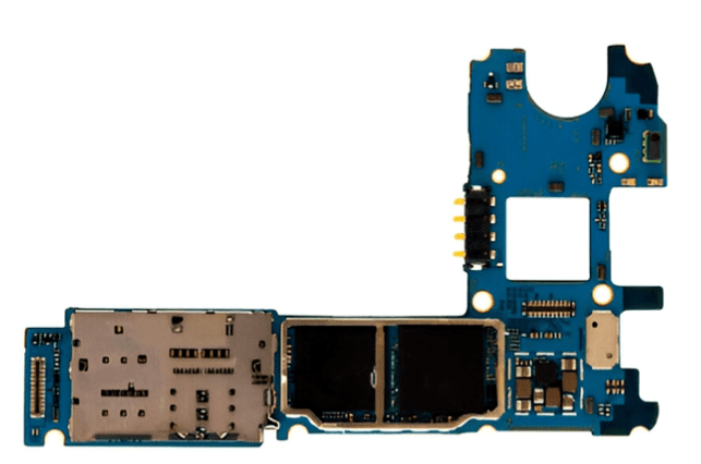
- Multi-Layer Boards have three or more conductive graphic layers, laminated together with insulating material in between. Multi-layer boards are the product of the development of electronic information technology towards high speed, multi-function, large capacity, small size, thin profile, and light weight. Currently, most complex electronic devices, such as smartphones and computer motherboards, use multi-layer board designs.
Classified by substrate characteristics, PCBs can be rigid boards, flexible boards, or rigid-flex boards.
- Rigid Boards use substrates that are not easily bent. Common PCBs are mostly rigid PCBs.
- Flexible Boards use soft insulating materials like PTFE or polyester as the substrate. They can be folded, bent, and rolled, enabling three-dimensional wiring in space.
- Rigid-Flex Boards are made by combining flexible substrate materials with rigid substrate materials in different areas. They are mainly used in the interface parts of printed circuit boards.
How PCBs Work
The working principle of a PCB is the result of the coordinated operation of all components and circuits. Each part plays a crucial role in the overall performance of the PCB. Power and signal distribution work independently, ultimately producing the desired output. Understanding how a PCB works is essential for design and troubleshooting. The following sections describe the working principles of the various parts of a PCB:
Electrical Continuity
Copper traces act as pathways for electrical signals, connecting all components on the board. When the PCB is powered on, the traces distribute power to each component and receive the output response. The trace network is perfectly designed without any gaps, breaks, crosses, or short circuits, and is evenly distributed across the entire PCB. This section clearly explains the principle of current flow in a PCB.
Signal Routing
The PCB board receives data signals from users and the external environment as input. These signals have independent traces and pin configurations from the power traces. Signals flow from these traces and are sent to processing components. After processing, the signal output is routed to the output section for user use. This routing mechanism is a key component of how PCBs work for data transmission.
Component Response
Each component has its unique characteristics and responds differently to power and signals. Resistors control current flow, capacitors store and release charge, inductors store and release magnetic fields, transistors act as switches or amplifiers, and microprocessors receive input signals, process them, and generate and store results. The selection of components depends on the response characteristics required by the PCB for the corresponding output.
Feedback Mechanism
Many PCBs incorporate feedback mechanisms to maintain their output and operation. Any deviation in output generation or internal processing is detected and corrected by additional circuits. Feedback is crucial for the long-term reliable operation of PCBs. Furthermore, PCBs are equipped with devices based on sensors and alarms to identify adverse external events. This regulatory loop provides another perspective for understanding how PCBs ensure stability.
The Design and Manufacturing Process of PCBs
The design and manufacturing of PCBs is a complex and precise process that requires multiple steps to complete.
PCB design typically includes four basic steps: schematic circuit design, generating a netlist, printed circuit board layout design, and generating printed circuit board reports.
- Schematic Circuit Design involves creating a logical connection diagram of the circuit.
- Generating a Netlist shows the connection relationships between the various components in the circuit.
- Printed Circuit Board Layout Design translates the schematic into the actual board layout.
- Generating Various Reports facilitates production.
The main manufacturing steps include: cutting, drilling, copper deposition, pattern transfer, plating, etching, solder mask application, silkscreen printing, surface finish, shaping, and testing.
During the manufacturing process, the substrate is made from insulating, heat-resistant, and not easily bent material. The fine line material visible on the surface is copper foil. Originally, copper foil covers the entire board, but during manufacturing, part of it is etched away. The remaining part forms a mesh of fine lines. These lines are called traces, and they are used to provide circuit connections for the components on the PCB.
The Key Role of PCBs in Electronic Devices
PCBs play an indispensable role in electronic devices, far beyond simple connections.
- Provides Mechanical Support: The PCB provides mechanical support for various electronic components. By soldering and fixing components onto the PCB, the stability and firmness of the electronic device are maintained.
- Enables Electrical Connection: Interconnects individual components through wiring to form a complete circuit function. Traces, copper layers, and vias collectively ensure reliable conduction of electrical current.
- Controls Electrical Performance: PCB design can optimize electrical performance, including signal integrity, impedance control, and filtering & shielding.
- Thermal Management: Electronic components operating at high power or high speed generate significant heat. PCBs undertake the critical role of heat dissipation and thermal management.
- Power Management: In electronic systems, PCBs not only conduct signals but also undertake the role of power distribution.
- Provides Identification and Test Points: Identifications, numbers, test points, and other information are printed on the PCB, facilitating subsequent debugging, testing, and maintenance.
Future Trends in PCB Development
With the continuous development of electronic technology, PCB technology is also advancing to meet the growing demands of electronic devices.
The design and manufacturing of PCBs are gradually moving towards multi-layer, multi-function, high-speed, and high-density directions. High-Density Interconnect (HDI) technology allows for finer lines and smaller spacing on PCBs.
Integrated Component PCBs embed passive components directly inside the PCB, saving space and improving performance.
Environmentally Friendly PCBs actively respond to environmental regulations by adopting lead-free and cadmium-free processes, reducing heavy metal pollution.
High-Speed/High-Frequency PCBs adapt to the needs of 5G and high-speed digital circuits, using materials with low dielectric constants.
Rigid-Flex Board technology combines the advantages of rigid and flexible boards, providing solutions for special applications.
Conclusion
The evolution of electronic technology continues to drive key innovations in PCB technology. The future of PCBs lies in High-Density Interconnect (HDI), flexible and stretchable circuit boards, embedded components, 3D printed circuit boards, and eco-friendly materials. Although the working principle of PCBs will still be based on logic circuits, their reliability and performance will be significantly enhanced.
For PCB engineers and end users, understanding how a PCB works is crucial for achieving optimal use. Exploring the world of PCBs is a fascinating and highly technical journey.


0 Comments