
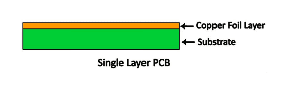
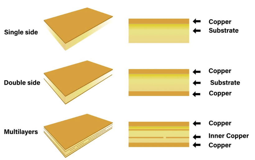
A single-layer PCB, also known as a single-sided PCB, is a specific type of printed circuit board. Its characteristic is that only one side of the board has a single layer of conductive material, while the other side is used for integrating various electronic components onto the board (the conductor pattern).
Typically, these single-layer boards consist of just one layer of conductive material, usually made from copper foil, which manufacturers etch to create the circuit pattern. It’s important to note that single-sided boards can be made from a variety of materials, offering multiple options to consider.
Aluminum substrates are known for their affordability and excellent thermal conductivity, performing exceptionally well in heat dissipation. FR-4 grade glass fiber laminate, made from glass fiber, offers both heat resistance and cost-effectiveness. CEM-1 and CEM-3, which use glass fiber and epoxy resin, are both economical choices with good heat resistance. Finally, copper-based single-layer PCBs use a thin copper foil laminated onto a dielectric substrate, excelling in applications requiring superior electrical and thermal conductivity. Each material has its unique advantages, effectively meeting specific project needs.
Single-layer PCBs are the foundation of PCB technology and still play a significant role in the electronics industry today. Furthermore, single-sided PCBs remain widely used in various applications, including those requiring low-cost electronic components.
Construction of a Single-Layer PCB
A single-layer PCB has only one conductive layer, but requires a base or substrate material to provide structural support.
The type and properties of this substrate determine the board’s application and flexibility/rigidity.
On the conductive layer, the foil thickness can vary depending on the application, and it can be defined in ounces per square foot.
The board also requires a solder mask layer over the copper traces to prevent corrosion, short circuits, and other failures.
The final layer in the stack is the silkscreen layer, which prints component designators, symbols, and values on the mounting surface to simplify the assembly process and aid in understanding the board’s operation.
Single-Layer PCB Design
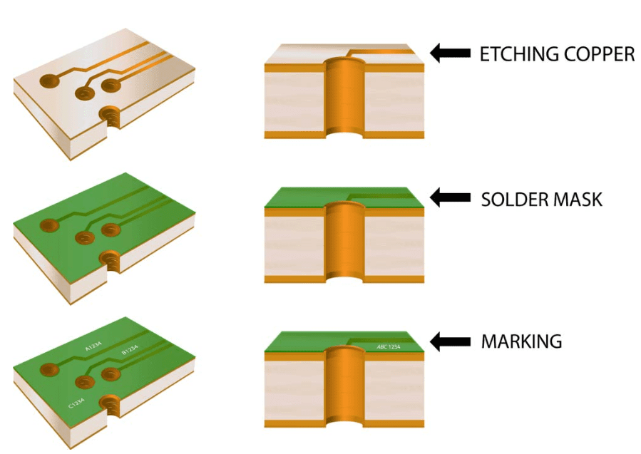
Because single-layer boards use only one conductive layer, the conductive paths cannot cross or overlap. The PCB’s base material, also called the substrate, is made from heat-insulating material, most commonly compacted glass fiber, which ensures the board’s strength and durability. The choice of substrate material depends on whether the board is flexible or rigid. The top of this substrate has a copper layer, which serves as the conductive path for the various components on the board. Different boards require different copper thicknesses, measured in ounces per square foot (oz/sq ft), and are adjusted based on different needs and expectations.
One side of the copper foil is coated with a solder mask layer to prevent accidental conduction and protect it from direct contact with other conductive materials. This thin solder mask layer acts as a crucial insulating barrier. The other side features the silkscreen layer, which sits on top of all other layers and is primarily used for printing characters and symbols on the board. This additional layer simplifies understanding the PCB, aiding in comprehending its function and identifying components.
The board is laminated with a metal layer; one side is for electrical connections of components, and the other is for mechanical attachment.
Types of Single-Layer PCBs
- Single-Layer Rigid PCB: This is a single-layer PCB made from rigid material like glass fiber. This type of board is not flexible but prevents circuit breaks and bending. Currently, they are used in various types of equipment, such as power supplies, calculators, etc.
- Single-Layer Flexible PCB: This is a single-layer PCB made from flexible materials like plastics instead of rigid ones. Single-layer flexible PCBs offer many advantages over single-layer rigid PCBs, but have a higher manufacturing cost.
- Single-Layer High-Frequency PCB: This type of single-layer PCB is typically used for high-frequency applications in the Gigahertz range. These PCBs are made from materials like Teflon or Polyphenylene Oxide (PPO). When selecting a high-frequency single-layer PCB, you need to understand factors like thermal expansion, dielectric loss, and water absorption.
- Single-Layer Rigid-Flex PCB: This is a single-layer PCB made from a combination of glass fiber and plastic. Therefore, the single layer is typically associated with both plastic and glass fiber. Compared to purely rigid or flexible single-layer PCBs, they offer advantages such as potentially reducing the overall size and weight of the PCB.
- Single-Layer Aluminum-Backed PCB: This is a single-layer PCB made with an aluminum material substrate. The design of this PCB is very similar to a copper-backed PCB, but the difference lies in its use of an aluminum PCB substrate instead of copper. This is because aluminum-backed PCBs require thermally conductive materials to transfer heat from the insulating material to the substrate.
Advantages of Single-Sided PCBs
- Simple and straightforward design, installation, and manufacturing process compared to double-sided or multi-layer PCBs.
- Lower cost, especially suitable for mass production. Single-layer PCBs are generally inexpensive to produce, making them an excellent alternative for low-density designs.
- Considered well-known, common, and easy to understand by most PCB manufacturers.
- Processes like drilling, soldering, desoldering, and component insertion on the board are easier because it consists of only one layer.
- Reduced probability of issues like short circuits and noise during manufacturing.
- Components are placed only on one layer, often requiring fewer or lower jumpers to correct the circuit.
- Less time required for fault diagnosis and repair.
Disadvantages of Single-Layer PCBs
- Limited to low pin-count devices or simple equipment.
- More susceptible to electromagnetic interference.
- Not suitable for high-speed or high-density circuits.
- Routing for complex circuits is more difficult.
- Limited to one side of the board, unlike double-sided or multi-layer PCBs.
Single-Layer PCB Thickness
The industry standard for PCB thickness is about 1.57 mm or 0.062 inches, but depending on its construction, it can range from 0.2 mm to 6.1 mm.
Lower thicknesses are usually for flexible boards, as the copper layer thickness is often standard for single-layer boards.
These boards typically lack vias or thick copper traces to handle high-frequency signals.
Therefore, changing the thickness of the substrate layer can make the PCB rigid or flexible.
Raw Materials for Single-Sided PCBs
- Aluminum: Aluminum is the most common raw material for single-layer PCBs, and aluminum substrates are also the cheapest. The main advantage of aluminum is its good thermal conductivity, allowing for rapid heat dissipation.
- FR-4 Grade Glass Fiber Laminate: FR-4 is a commonly used dielectric in single-sided PCBs. FR stands for Flame Retardant, and it is made from glass fiber. The main advantages of FR-4 are its good heat resistance and lower cost compared to other dielectrics.
- CEM-1: CEM-1 is a low-cost material for single-layer PCBs. It uses glass fiber and epoxy resin. The main advantages of CEM-1 are its good heat resistance and lower cost compared to other dielectrics.
- CEM-3: The main materials for CEM-3 are glass fiber and epoxy resin. It is a single-sided PCB with good heat resistance. The main advantage of CEM-3 is its good heat resistance and lower cost compared to other dielectric materials.
- Copper-Based: Copper single-layer boards use a thin layer of copper foil laminated onto a dielectric substrate.
The main advantages of copper single-layer boards are excellent electrical and thermal conductivity.
Typically, copper single-layer PCBs are suitable for high-power applications where heat dissipation is a consideration.
What is the Difference Between Single-Layer and Multi-Layer PCBs?
The difference between single-layer and multi-layer PCBs is crucial for determining their applications, complexity, and cost. The basic design of a single-layer or single-sided PCB involves having only one layer of conductive material (typically copper) covering one side of the board. The other side is usually covered with a non-conductive substrate, often made of glass fiber or other insulating material. Due to their simple construction, these PCBs are the preferred choice for hobbyists and students.
On the other hand, multi-layer PCBs are distinctly different. These boards contain two or more layers of conductive elements, which are sandwiched between insulating layers, allowing for greater routing space and component placement. Consequently, they are well-suited for more complex projects or electronic devices where space is limited and circuits are intricate.
One of the most significant advantages of multi-layer PCBs is their ability to incorporate ground planes or ground grids, effectively reducing electrical noise. Traces can cross over each other simply by having one trace go below the board and re-emerge on the top, simplifying the design process.
While multi-layer PCBs offer greater design freedom and complexity, they also come with increased complexity and cost. These boards are typically used in high-end electronics, such as sophisticated smartphones, which feature multiple layers to support complex circuitry where performance and compactness are paramount.
Single-Layer PCB Applications
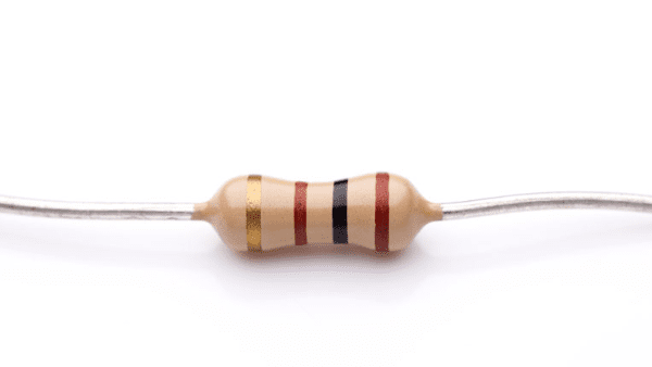
Resistors
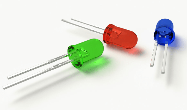
Diodes
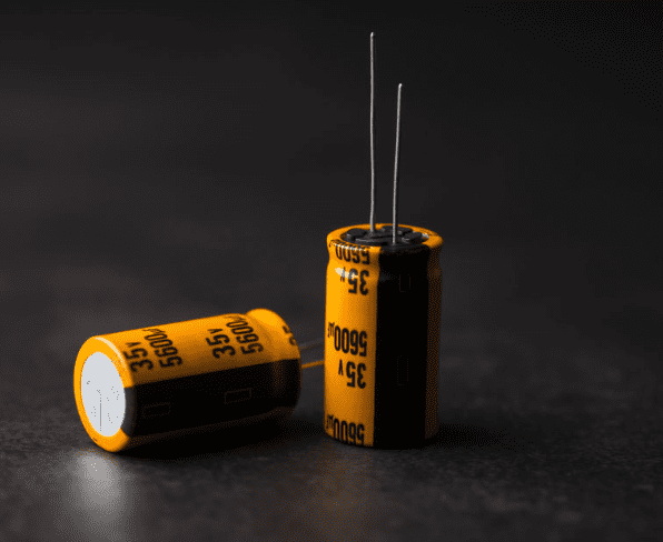
Capacitors
Switches

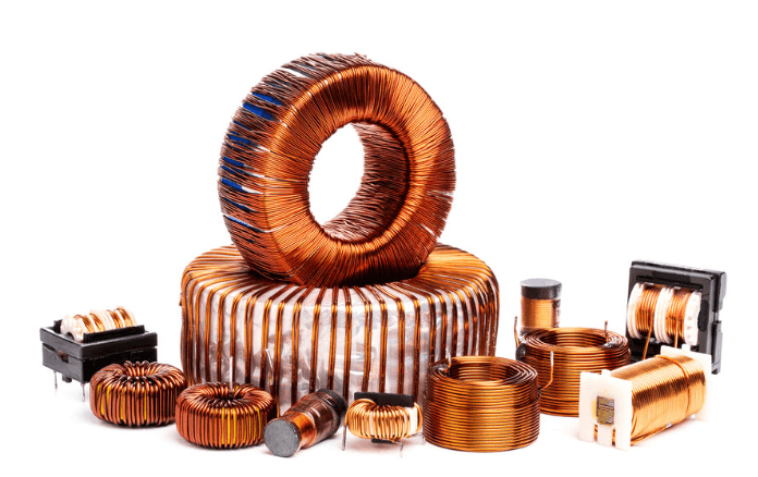
Inductors
Single-Layer PCB Design
Single-layer board design refers to the process of designing a printed circuit board with only one conductive layer. Here are some tips for single-layer board design:
- Keep the design as simple as possible.
- Use wide traces for power and ground lines.
- Use vias judiciously.
- Keep the board size as small as possible.
- Use a ground plane if possible.
- Keep trace lengths as short as possible.
- Avoid using buried or blind vias.
If you need assistance with single-layer design, contact an experienced PCB designer. They can help you overcome the challenges of single-layer circuit design and ensure your board is manufactured to the highest quality standards.

Summary
The single-layer PCB is like the “sketchpad” of electronic engineering – it is simple, straightforward, and economical, serving as the starting point for countless classic designs and introductory projects. It may not carry the complex “intelligence” of modern smartphones or supercomputers, but in cost-sensitive, functionally specific applications, it still plays an irreplaceable role. Understanding single-layer PCBs is not only the first step in learning PCB knowledge but also an excellent example for understanding how to balance cost, performance, and complexity in engineering design. In today’s pursuit of extreme integration, this simple green board still quietly supports a vast number of basic electronic devices in our daily lives.


0 Comments