
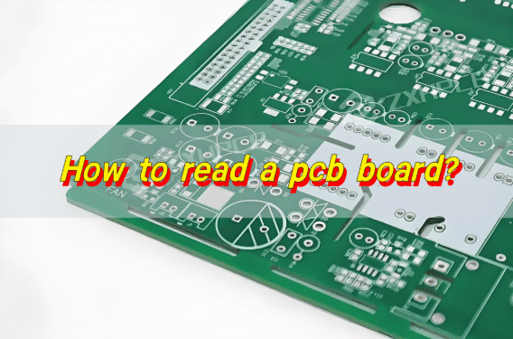
Inside every electronic device we use daily lies a meticulously planned “miniature city” — the Printed Circuit Board (PCB). The crisscrossing copper traces are its “roads,” the various electronic components are its “buildings,” and the flowing electrical currents and signals are the ceaseless “traffic.” Learning to read a PCB is like obtaining an engineering map of this city, allowing you to understand its operational secrets. This is an extremely critical skill, whether for learning, debugging, or repair.
This article will guide you step-by-step, from the basics to advanced levels, in mastering the art of interpreting PCBs.
Define Your Objective: What Level of “Understanding” Are You Aiming For?
“Understanding” exists on different levels. Defining your goal provides clear direction:
- Beginner: Identify major components and basic functions.
- Can distinguish resistors, capacitors, inductors, diodes, transistors, integrated circuits (ICs), etc.
- Can roughly determine the board’s primary function (e.g., power supply board, motor driver board, audio amplifier).
- Intermediate: Understand signal flow and functional modules.
- Can partition the board into different functional blocks (e.g., power supply section, MCU core section, sensor interfaces, communication interfaces).
- Can understand how signals (data) flow across the board.
- Advanced: Understand the complete circuit schematic and perform debugging and repair.
- Can reference the schematic diagram to understand the specific role of every component.
- Can analyze fault points and perform measurements and repairs.
The Four-Step Process to Reading a PCB
This is a process that moves from the macro to the micro, from the surface to the essence.
Step 1: Macro Observation and Information Gathering
- Observe the Overall Layout:
- Examine the board’s size, shape, and number of layers (often indicated by thickness and whether vias go through all layers).
- Identify the main connectors (e.g., power jack, USB, Ethernet port, display ribbon cable socket). These are the board’s windows to the outside world and provide direct clues to its function.
- Look for the “Identification Card”:
- Board Number/Model: Typically found on the silkscreen (white text and graphics) in formats like
MB-102, REV 1.2. Use this to search online for schematics or documentation. - Main Chips: Locate the largest chips with the most pins. Note their part numbers (e.g.,
STM32F103C8T6,ATMEGA328P,LM2596). These are the “brain” and “heart” of the board, defining its core functionality.
- Board Number/Model: Typically found on the silkscreen (white text and graphics) in formats like
- Identify Functional Areas:
- Power Area: Usually contains large electrolytic capacitors, inductors, and power management ICs. Input/output sections often have fuses, bridge rectifiers, etc.
- Core Processing Area: Centered around the main MCU/CPU, typically featuring a crystal oscillator (a metal-cased cylinder or rectangle with two small capacitors nearby), a reset circuit, and configuration resistors/capacitors.
- Interface/Driver Area: Near the connectors, you’ll often find level-shifter chips, isolation optocouplers, and driver ICs (e.g., for motors or LEDs).
- Analog/Digital Isolation Area: Sometimes marked by a visible “moat” or a row of isolation components, separating analog sections (e.g., op-amps, sensor signal conditioning) from digital sections to reduce interference.
Step 2: Know the Basic “Inhabitants” – Electronic Components
This is the foundation of reading a PCB. You must be familiar with the appearance, symbols, and functions of common components.
| Component | PCB Silkscreen Symbol / Appearance | Primary Function | Remarks |
|---|---|---|---|
| Resistor | “R” prefix, color bands or number code | Limit current, divide voltage | Most fundamental component |
| Capacitor | “C” prefix, typically block-shaped or disc-shaped | Filtering, energy storage, coupling, block DC | Note polarity (electrolytic caps have a negative marker) |
| Inductor | “L” prefix, typically coil-shaped or a bead | Filtering (especially high frequencies), energy storage | Common in power circuits |
| Diode | “D” prefix, has polarity marking | Rectification, freewheeling, voltage regulation, reverse polarity protection | Directional; the cathode is marked with a line on the silkscreen |
| LED | “LED” or “D” prefix, has polarity marking | Light emission for indication | Long leg is anode; silkscreen may show a light-emitting shape |
| Transistor / MOSFET | “Q” or “T” prefix, typically three pins | Switching, amplification | Distinguish between NPN/PNP or N-MOS/P-MOS |
| Integrated Circuit (IC) | “U” or “IC” prefix, multiple pins | Implements complex functions | The key is understanding its datasheet |
Pro Tip: The silkscreen (white text) on the PCB is a crucial clue:
- R for Resistor, C for Capacitor, L for Inductor, D for Diode, Q for Transistor/MOSFET, U for Integrated Circuit, J or P for Connector.
- Component designators like R1, C2 help you locate parts in the schematic.
Step 3: Trace the “Roads” – Copper Traces
The essence of a PCB is connecting components through copper traces.
- Distinguish Trace Types:
- Power Traces: Usually wider and thicker, as they need to carry higher current.
- Ground (GND) Traces: Also relatively wide; sometimes implemented as a large-area copper pour.
- Signal Traces: Typically thinner, especially for high-speed digital or analog signals.
- Learn the “Traffic Rules”:
- Vias: “Overpasses” that connect traces on different layers.
- Teardrops: Reinforcing fillets at the junction of a pad and a trace, shaped like a teardrop.
- Copper Pour: Large areas of copper, usually connected to ground, used for shielding and improving EMC.
- Use a Multimeter:
- Set the multimeter to the continuity or resistance mode to trace connectivity. This is the most critical tool for verifying your hypotheses without a schematic.
Step 4: Correlate with the Schematic Diagram (If Possible)
Finding the schematic for the board (or its core chips) online represents a qualitative leap in understanding.
- Cross-Reference: Find a component (e.g., C15) in the schematic and then locate its physical position on the PCB, observing its connections.
- Understand Nets: A connection in the schematic corresponds to the same “net” on the PCB. The ability to highlight a net in EDA software (like KiCad, Altium) is extremely powerful.
- Signal Flow Analysis: Start from an input connector and follow the schematic, tracing the signal’s entire path on the PCB to see what processing it undergoes and where it ultimately goes.
Core Mindset: Divide and Conquer – The Functional Block Method
This is the key to understanding complex PCBs. Don’t try to comprehend everything at once.
View the entire board as a system and break it down into independent functional modules:
- Power Supply Module:
- Questions: Where does power enter? Is it AC or DC? What is the voltage?
- Path: Input -> Filtering/Protection -> Voltage Conversion (DC-DC or LDO) -> Output to various sections.
- Components: Fuses, bridge rectifiers, large capacitors, power ICs, inductors, filter capacitors.
- Main Control Module:
- Core: MCU/CPU/FPGA.
- Essential Peripherals: Crystal oscillator (clock), reset circuit, Boot configuration circuit, decoupling capacitors.
- Input Module:
- What is it?: Buttons, sensors, ADC sampling circuits.
- Path: External Signal -> Interface -> Signal Conditioning (e.g., pull-up resistors, filtering) -> Main Controller.
- Output Module:
- What is it?: LED indicators, displays, relays, motors, speakers.
- Path: Main Controller -> Driver Circuit (e.g., transistors, MOSFETs, driver ICs) -> Load.
- Communication Module:
- What is it?: UART, I2C, SPI, USB, Ethernet, etc.
- Path: Main Controller <-> Level Shifting/Isolation/PHY Chip <-> External Interface.
After analyzing each module, consider how they work together.
Practical Advice and Tools
- Start with Simple Boards: For example, a minimal 51-MCU system board or an LM317 voltage regulator board. Successfully analyzing a simple board builds great confidence.
- Leverage Search Engines and Datasheets: Immediately search for the datasheet of any unfamiliar chip. Datasheets usually include typical application circuits, which are often the direct answer for that section of your circuit.
- Use a Magnifying Glass and Good Lighting: Protect your eyesight and see the details clearly.
- Learn to Use EDA Software: Even free versions like KiCad or online tools like EasyEDA. Opening open-source projects and viewing both the schematic and PCB layout is the fastest way to learn.
- Practice Hands-On Measurement: Power up the board (with caution!) and use a multimeter to measure voltages at key points (e.g., input/output of power chips). Use an oscilloscope to view waveforms. Combine theory with practice.
How to Determine the Number of Layers in a PCB
To determine the number of layers in a Printed Circuit Board (PCB), you can employ the following methods:
- Inspect the Edge: Carefully examine the PCB’s edge. If you can see multiple layers of copper foil or laminate, it is likely a multilayer PCB. Each distinct copper layer represents a separate signal or plane layer.
- Count the Vias: Multilayer PCBs typically have a higher density of vias. Observe the pattern of holes on the PCB surface. If you notice many vias that do not appear to go straight through the board, it suggests internal layers are being connected.
- Examine the Board Thickness and Build-Up: Simple 1 or 2-layer boards are often thinner. A noticeably thicker board often indicates more internal layers.
- Look for Printed Markings: PCB manufacturers often include a layer count designation in the silkscreen or as an etched marking. Look for identifiers like
4L,6L, etc. - Hold to a Light Source: With a strong backlight, you can sometimes see the internal trace patterns of the inner layers, allowing you to infer the layer count.
How to Identify PCB Substrate Material
- Visual and Tactile Inspection:
- Color: The common green or brown color typically indicates FR-4 fiberglass. A white, hard, and brittle material may be a ceramic substrate. A silver color with a metallic feel suggests an aluminum core (metal-core PCB or MCPCB). Note that black PCBs sometimes feature special coatings or materials for enhanced EMI performance.
- Texture and Flex: FR-4 is rigid and has a specific fiberglass feel. Ceramic is very hard and brittle. Aluminum core boards are unmistakably metallic and heavy for their size.
- Consider the Application and Environment:
- High-Temperature Environments: Applications like automotive engine controls or industrial furnaces may use high-Tg FR-4, ceramic, or metal-core substrates for better heat dissipation (e.g., aluminum substrates in EV motor controllers).
- High-Frequency Circuits: RF applications, such as 5G communication equipment and radar systems, require materials with low dielectric loss, such as Polytetrafluoroethylene (PTFE/Teflon) based substrates.
- High-Power/Current Applications: These often use boards with thicker copper weights or metal cores for improved current carrying and thermal management.
- Check Markings and Documentation:
- PCB Markings: Look for manufacturer logos, UL certification marks, or material type codes printed on the silkscreen.
- Product Documentation: Consult the board’s datasheet, technical manual, or Bill of Materials (BOM), which may specify the substrate material (e.g., “FR-4,” “Rogers 4350B”).
Silkscreen Annotations
Silkscreen annotations are crucial elements in PCB design, providing visual guidance for component placement, orientation, and identification. These markings, typically printed in white or yellow ink on the PCB’s top layer, contrast with the board color for easy reading.
The primary purpose of silkscreen annotations is to facilitate PCB assembly, testing, and troubleshooting. They offer an intuitive reference for technicians and engineers, enabling them to quickly identify components and their characteristics without constantly consulting schematics or datasheets.
Common types of silkscreen markings include:
- Component Outlines: Simplified drawings indicating a component’s shape and size, aiding correct placement during assembly.
- Reference Designators: Alphanumeric codes (e.g.,
R1for Resistor 1,C4for Capacitor 4) that uniquely identify each component on the board. - Polarity Indicators: Symbols or markings showing the correct orientation for polarized components like electrolytic capacitors or diodes.
- Pin 1 Indicators: A dot, notch, or other mark used to identify the first pin of an integrated circuit or other multi-pin component.
- Test Points: Marked locations on the board for probing during quality control or troubleshooting.
- Logos and Board Information: Manufacturer logos, board revision numbers, and date codes are often included in the silkscreen layer.
Common silkscreen annotations and their meanings:
+Symbol: Indicates the positive terminal of a polarized component.- Diode Symbol (
▷|): Shows the direction of current flow for a diode. - GND: Denotes a ground connection point.
- VCC or VDD: Indicates a power supply rail.
Best Practices for Interpreting Silkscreen Information:
- Familiarize yourself with standard component symbols and abbreviations used in PCB design.
- Cross-reference silkscreen annotations with the schematic when available.
- Pay close attention to polarity indicators, especially for components like electrolytic capacitors and diodes.
- Use reference designators to quickly locate specific components during troubleshooting.
- Be aware that silkscreen may be omitted or incomplete on prototypes or cost-optimized boards.
- Consult the component datasheet if there is any doubt about orientation.
- Remember that silkscreen can wear off over time, especially in harsh environments.
By understanding and effectively utilizing silkscreen annotations, engineers and technicians can significantly improve the efficiency of PCB assembly, testing, and debugging processes.
Using a Multimeter and Continuity Tester
Multimeters and continuity testers are indispensable tools for tracing circuits and verifying connections on a PCB. They help engineers confirm electrical pathways between components, identify short circuits, and locate open circuits.
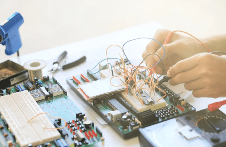
Continuity testing works on the principle that a closed circuit with low resistance allows current to flow, while an open circuit or a high-resistance path does not. Most modern digital multimeters (DMMs) include a continuity function, which typically emits an audible beep when a connection is detected.
To use a multimeter for tracing circuits on a PCB, follow these steps:
- Ensure the multimeter is set to the “Continuity” mode (diode/speaker symbol) or a low resistance (Ω) setting.
- Ensure the circuit is completely powered off to prevent electric shock or meter damage.
- Insert the black probe into the COM jack and the red probe into the VΩmA jack.
- Place the black probe on one point of the circuit you want to check.
- Touch the red probe to another point in the circuit.
- Observe the multimeter: a beep or a very low resistance reading (near 0Ω) indicates continuity. No beep or a high reading (OL – Open Loop) indicates no connection.
- Repeat the process for other points as needed.
- Turn off the multimeter and remove the probes after testing.
Critical Safety and Best Practices:
- Always power down the circuit before performing continuity tests.
- Use insulated probes and keep your hands dry.
- Wear safety glasses to protect against potential sparks or debris.
- Be aware that capacitors can retain a charge even after power is removed.
- Use a multimeter rated for the voltage levels you might encounter.
- Avoid touching exposed conductors or components on a live circuit.
- Use one hand to probe live circuits when absolutely necessary to minimize current path across the chest.
- Keep your work area clean and organized to prevent accidental shorts.
By mastering the use of multimeters and continuity testers, engineers can efficiently trace circuits, verify connections, and troubleshoot PCB issues with confidence and precision.
Thermal Management Considerations
Thermal management is a critical aspect of PCB design, directly impacting the performance, reliability, and lifespan of electronic components. Proper thermal management prevents overheating, reduces thermal stress on components, and ensures consistent performance under varying environmental conditions.
Identifying thermal management features on a PCB involves recognizing specific patterns and components designed for heat dissipation:
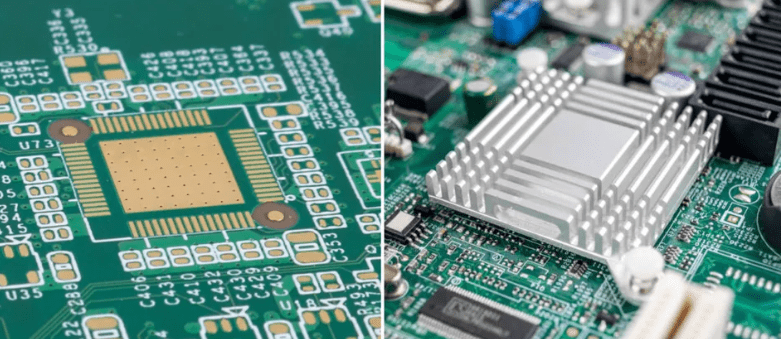
- Thermal Relief Pads: These are spoke-like connections between a pad and the surrounding copper pour. They balance solderability (by reducing heat sinking during soldering) with thermal conductivity during operation.
- Heat Sinks: These are metal structures, often finned, attached to high-power components. On the PCB, look for mounting holes or large pads near high-power ICs or regulators.
- Thermal Vias: These are arrays of small vias placed under or near heat-generating components. They conduct heat to other layers or the opposite side of the board.
- Copper Pour: Large, continuous areas of copper on power and ground planes aid in spreading heat. This is often visible on the outer layers of the PCB.
- Component Spacing: Observe the layout for adequate spacing between heat-generating components to allow for better airflow.
The table below compares different thermal management techniques and their visual indicators on a PCB:
| Technique | Visual Indicator | Effectiveness | Typical Applications |
|---|---|---|---|
| Thermal Relief | Spoke-like connections to pads | Moderate | General purpose, for soldering pads connected to pours |
| Heat Sink | Large metal structure/mounting points | High | Processors, Power Amplifiers, High-power components |
| Thermal Vias | Clusters of small vias near components | Medium to High | BGA packages, high-power LEDs |
| Copper Pour | Large continuous copper areas | Moderate | Power/Ground planes, general heat spreading |
| Component Spacing | Deliberate gaps between components | Low to Moderate | Air-cooled designs |
| Thick Copper | Similar appearance, may feel heavier | High | High-current applications |
| Thermal Pads/Interface | Colored material between component/PCB | High | Interface between component and heat sink |
| Conformal Coating | Thin, even coating on PCB surface | Low | Environmental protection, minor thermal distribution |
Understanding these techniques and their visual indicators enables engineers to quickly assess a PCB’s thermal design and identify potential areas for improvement. This knowledge is essential for optimizing circuit performance, enhancing reliability, and extending the service life of electronic devices.
Conclusion
Learning to read a PCB is an accumulative process, much like learning a new language. You start by recognizing a few “words” (components), then learn the “grammar” (circuit principles), until finally you can read the entire “essay” (the PCB board).
Remember the workflow:
Observe the whole -> Identify components -> Partition into modules -> Trace the tracks -> Correlate with the schematic -> Understand the system.


0 Comments