
1. Introduction
The Printed Circuit Board (PCB) is the backbone of modern electronic devices, interconnecting various electronic components to form a complete functional system. A PCB trace is the conductive copper pathway etched onto the insulating substrate of a PCB, responsible for transmitting electrical signals and power between components. It can be imagined as the “highway system” of the electronic world, where current and data signals travel along these “roads” between “cities” (components) like chips, resistors, and capacitors. Without efficient and reliable traces, no complex circuit design can realize its intended function.
The quality of PCB traces directly determines the performance, reliability, and stability of the entire electronic product. Poor trace design can lead to a series of issues, including signal integrity degradation, crosstalk, excessive electromagnetic interference (EMI), compromised power integrity, and overheating. Therefore, a deep understanding of the principles, design rules, and manufacturing processes of PCB traces is an indispensable core skill for electronics engineers, PCB designers, and hardware enthusiasts. This guide will provide a comprehensive analysis of all aspects of PCB traces, from fundamental materials to key parameters, and on to advanced design and repair techniques, offering a complete reference manual.

2. Materials and Construction of PCB Traces
A PCB trace is not an independent wire but an integral part of the PCB laminated structure. Its performance and manufacturing process are intrinsically linked to the materials used.
Substrate Materials:
The substrate is the insulator that supports the traces, and its material selection is critical.
- FR-4: This is the most commonly used substrate material, a glass fiber-reinforced epoxy laminate. It offers good mechanical strength, heat resistance, and electrical insulation properties at a low cost, making it suitable for the vast majority of consumer electronics and industrial products. Its typical Glass Transition Temperature (Tg) ranges between 130°C and 180°C.
- High-Frequency Materials: When operating frequencies enter the Radio Frequency (RF) and microwave domains (e.g., GHz range), the dielectric loss (Df) of FR-4 becomes excessively high, leading to severe signal attenuation. In such cases, high-frequency laminates produced by companies like Rogers or Taconic (e.g., RO4003C) are required. These materials possess a lower and more stable Dielectric Constant (Dk) and very low loss factors, ensuring high-frequency signal integrity.
- Flexible Materials: For Flexible Printed Circuits (FPCs), the substrate uses flexible films such as Polyimide or Polyester (PET). Polyimide offers high-temperature resistance and excellent flex endurance, making it common for connections requiring repeated bending.
Conductive Material:
- Electrodeposited Copper Foil: The primary material for traces is copper, chosen for its high conductivity, moderate cost, and ease of processing. During manufacturing, copper foil is laminated onto the substrate under heat and pressure. The initial foil thickness is typically specified in ounces per square foot (oz/ft²). The most common weight is 1oz copper, which corresponds to a thickness of approximately 35 micrometers (μm).
Surface Finish:
To prevent the oxidation of copper traces in air and ensure good solderability, a protective coating is applied to the trace surfaces.
- Hot Air Solder Leveling (HASL): A traditional process, low cost, but results in an uneven surface unsuitable for fine-pitch components.
- Electroless Nickel Immersion Gold (ENIG): Provides a flat surface, strong oxidation resistance, good solderability, and contact properties, making it a current mainstream choice.
- Immersion Silver and Organic Solderability Preservative (OSP): Other available processes, each with its own cost and performance trade-offs.
| Material Type | Primary Composition/Description | Advantages | Disadvantages/Typical Applications |
|---|---|---|---|
| Substrate – FR-4 | Glass Fiber Epoxy Resin | Low cost, good mechanical strength, versatile | High high-frequency loss, General-purpose electronics |
| Substrate – High-Freq | Ceramic-filled PTFE, etc. | Stable dielectric constant, very low loss | High cost, RF/Microwave circuits |
| Substrate – Flexible | Polyimide | Bendable, high heat resistance | High cost, lower mechanical strength, Wearable devices |
| Conductor – Copper | Electrodeposited Copper Foil | Good conductivity, easy to etch | Prone to oxidation when exposed to air |
| Finish – HASL | Tin-Lead Alloy | Low cost, repairable | Uneven surface, not suitable for fine-pitch leads |
| Finish – ENIG | Nickel/Gold Layer | Flat surface, oxidation resistant, good solderability | Higher cost, potential “Black Pad” issue |
3. Trace Width: The Determinant of Current Carrying Capacity
Trace width is one of the most critical parameters in trace design, as it directly determines the amount of current a trace can safely carry. Current flowing through a trace generates Joule heating. If a trace is too narrow, its resistance becomes excessive, leading to overheating, which can cause copper delamination, burning, and even fire hazards.
Theoretical Basis and Calculation:
Current carrying capacity (ampacity) primarily depends on the cross-sectional area of the trace (width multiplied by thickness) and the permissible temperature rise (typically 10°C or 20°C above ambient temperature). The industry widely uses formulas or charts based on the IPC-2152 standard for these calculations.
A simplified empirical formula (for external traces, 10°C temperature rise) is:
I = k * ΔT^0.44 * A^0.725
Where:
- I = Maximum Current (Amperes, A)
- k = Correction Factor (approximately 0.048 for external traces)
- ΔT = Temperature Rise (Degrees Celsius, °C)
- A = Cross-sectional Area of Trace (Square Mils, mil²)
In practical engineering, designers more frequently use online calculators or predefined tables. The table below provides a simplified reference based on IPC-2152 (for 1oz copper thickness, external traces, 20°C temperature rise):
| Trace Width (mil) | Current Carrying Capacity (A) |
|---|---|
| 10 mil | 1.0 A |
| 20 mil | 1.8 A |
| 50 mil | 3.5 A |
| 100 mil | 6.0 A |
Example:
Assume a power module needs to supply a continuous 2A current to a load. According to the table above, using 1oz copper thickness, the external trace width should be at least 20 mils (approx. 0.5mm) to ensure safety. To provide a margin, a designer might choose a 30 mil or wider trace.
Design Considerations:
- Power Traces vs. Signal Traces: Power traces typically carry higher currents and require wider designs; signal traces carry very small currents (milliamps) and their width is primarily determined by manufacturing capabilities and impedance requirements.
- Internal Layer Traces: Due to poorer heat dissipation, the current carrying capacity of internal layer traces is typically lower than that of external traces of the same width, often requiring an additional 20%-50% width increase.
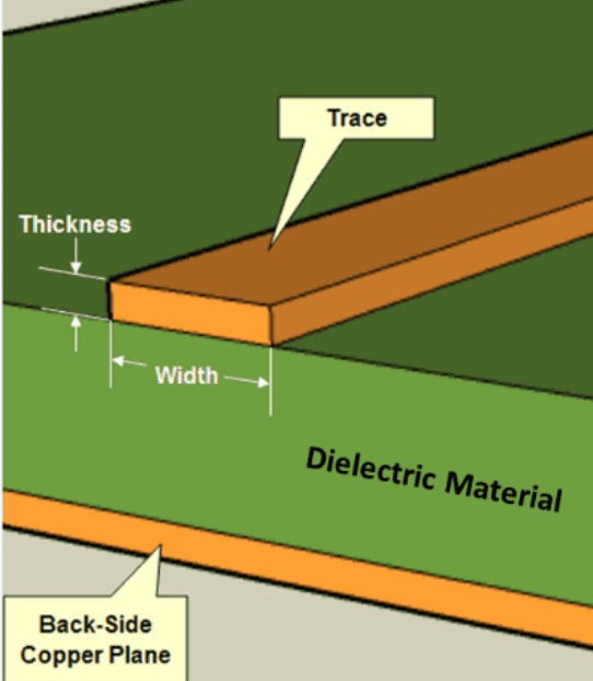
4. Trace Thickness: Copper Weight and DC Resistance
Trace thickness is likewise determined by the copper foil weight. Together with trace width, it defines the current-carrying cross-section. Trace thickness directly affects its DC resistance, which in turn influences voltage drop and power dissipation.
Copper Weight and Thickness Conversion:
- 1 oz Copper: Indicates that the copper foil weighs 1 ounce per square foot. Its thickness is approximately 1.4 mil or 35 μm.
- 0.5 oz Copper: Half the thickness, approx. 0.7 mil or 17.5 μm, often used in high-density boards.
- 2 oz Copper: Double the thickness, approx. 2.8 mil or 70 μm, commonly used in high-current power circuits.
DC Resistance Calculation:
The DC resistance of a trace can be estimated using the following formula:
R = ρ * L / (W * T)
Where:
- R = Trace Resistance (Ohms, Ω)
- ρ = Resistivity of Copper (approx. 1.7×10⁻⁶ Ω·cm)
- L = Trace Length (Centimeters, cm)
- W = Trace Width (Centimeters, cm)
- T = Trace Thickness (Centimeters, cm)
Example:
A trace with a length of 10cm, width of 0.5mm (0.05cm), and thickness of 1oz (0.0035cm) has a resistance of approximately:
R = (1.7e-6) * 10 / (0.05 * 0.0035) ≈ 0.097 Ω
When carrying a 1A current, the voltage drop across it is V = I * R = 0.097V, and the power dissipated is P = I² * R = 0.097W. For low-level signals or long-distance power distribution, this voltage drop and power loss may be significant.
5. Characteristic Impedance: The Core of High-Speed Digital and RF Circuits
When the signal rise/fall time is very short (i.e., rich in high-frequency components), or the trace length is comparable to the signal wavelength, a PCB trace can no longer be treated as a simple wire but must be considered a transmission line. At this point, matching the Characteristic Impedance becomes the primary task for ensuring signal integrity.
What is Characteristic Impedance?
Characteristic Impedance is the instantaneous impedance experienced by a signal as it propagates along a transmission line. It is determined by the trace’s geometry, dielectric material, and surrounding environment. The fundamental formula involves:
Z₀ = √(L/C)
Where L and C are the inductance and capacitance per unit length of the transmission line, respectively.
Factors Affecting Characteristic Impedance:
- Dielectric Constant (Dk, εr): An inherent property of the substrate material. A higher Dk increases capacitance C, thus lowering impedance Z₀.
- Trace Width (W): A wider trace increases capacitance C, lowering impedance Z₀.
- Trace Thickness (T): A thicker trace increases capacitance C, lowering impedance Z₀.
- Dielectric Thickness (H): The distance between the trace and the reference plane (usually ground). A greater H decreases capacitance C, raising impedance Z₀.
- Solder Mask: The solder mask covering the trace also has a dielectric constant and will slightly lower the impedance.
Common Transmission Line Structures:
- Microstrip: The trace is on an outer layer with one reference plane. It is categorized as “covered microstrip” (with solder mask) or “surface microstrip” (without).
- Stripline: The trace is embedded entirely within an inner layer, with reference planes above and below. It is less susceptible to external interference and offers more controlled impedance, but is more complex to route.
Impedance Control:
For high-speed interfaces (e.g., USB, HDMI, DDR, PCIe), the characteristic impedance of the source, trace, and load must be matched (typically 50Ω single-ended, 90Ω or 100Ω differential). Mismatches cause signal reflections, leading to overshoot, undershoot, and ringing, which can result in data errors. Designers use impedance calculation tools (e.g., Polar Si9000) to precisely calculate the required trace width based on the PCB fabricator’s stack-up and specify impedance control during manufacturing.
6. Fundamental Principles and Best Practices for PCB Trace Routing
Excellent trace routing is a blend of art and science. Below are several proven fundamental principles:
1. Routing Priority:
- Power and Ground First: Route power and ground networks first to ensure a low-impedance, low-noise Power Distribution Network (PDN).
- Critical Signals Next: Route sensitive signals like clocks, high-speed differential pairs, and reset lines next, providing them with optimal paths and protection.
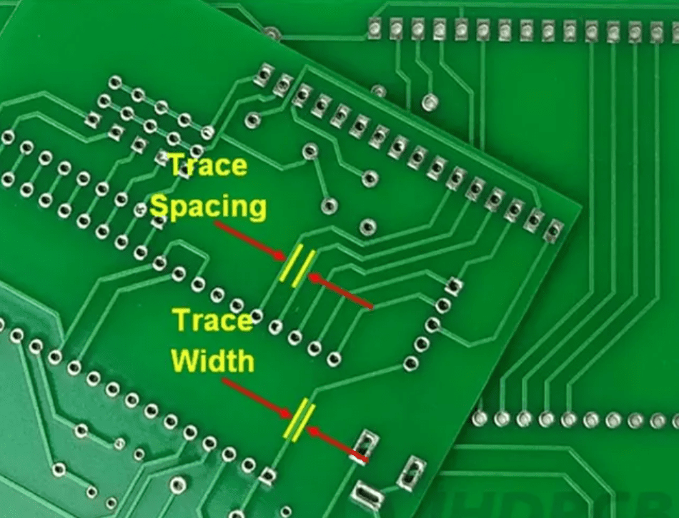
2. The 3W Rule:
To reduce crosstalk between parallel traces, the center-to-center spacing of adjacent traces should be at least 3 times the trace width (W). For example, for a 5mil wide trace, the spacing should be at least 15mil.
3. Minimize Return Path:
Current always returns to the source via the path of least impedance. For high-speed signals, the return current flows directly in the reference plane (usually the ground plane) underneath the signal trace. Therefore, one must never place cuts or splits in the reference plane underneath a critical signal trace. Forcing the return current to take a long detour creates a large current loop, dramatically increasing EMI and inductance.
4. Avoid Acute Angles:
In high-speed circuits, traces should turn using 45-degree angles or arc corners. Acute angles (90-degree corners) cause an effective increase in trace width at the corner, leading to an discontinuity in characteristic impedance and subsequent signal reflections. Additionally, during manufacturing, acid can trap in sharp corners, leading to over-etching.
5. Differential Pair Routing:
For differential signals (e.g., USB, HDMI), the traces must be strictly length-matched, equal in width, equally spaced, and tightly coupled. Length mismatch causes timing skew and reduces common-mode noise rejection.
7. Trace Repair and Debugging Techniques
Even after careful design and manufacturing, PCB traces can be damaged due to physical stress, overcurrent, or design flaws. Mastering repair techniques is crucial.
Common Failure Types:
- Trace Break: Caused by physical flexing, impact, or overcurrent burnout.
- Lifted Pad: Caused by repeated soldering/desoldering or thermal stress, detaching the component connection pad from the substrate.
- Short Circuit: Caused by solder bridges, conductive debris, or manufacturing defects connecting two isolated traces.
Repair Tools and Materials:
- High-Precision Temperature-Controlled Soldering Iron: Fine tip required.
- Low-Temperature Solder Wire: Leaded or lead-free, 0.3mm-0.5mm diameter preferred.
- Flux: Improves solder quality.
- Jumper Wire: Very fine insulated wire (e.g., AWG 30-40).
- Conductive Epoxy: For situations where heat cannot be applied.
- Microscope: Essential for high-density boards.
Repair Steps (Example: Broken Trace):
- Diagnosis and Preparation: Use a multimeter to confirm the break location. Gently scrape off the solder mask from both ends of the break using a knife or fine sandpaper to expose shiny copper.
- Tinning: Apply a small amount of flux to the exposed copper and use the soldering iron to coat it with a thin layer of solder.
- Bridging the Gap:
- Method A (Direct Solder Bridge): If the gap is very small (<1mm), it can be filled directly with solder to form a “solder bridge.”
- Method B (Jumper Wire): For longer breaks, take a piece of jumper wire, pre-tin both ends. Solder each end of the wire to the exposed, tinned copper points at either side of the break. Ensure a solid connection.
- Cleaning and Insulation: Clean flux residue with isopropyl alcohol. Insulate the repaired area by applying a drop of solder mask (UV-curable) or using a small piece of tape to prevent short circuits.
Precautions:
- Always ensure the PCB is powered off during repair.
- Control soldering iron temperature and time to avoid damaging nearby components or causing further copper peeling.
- Always perform continuity and insulation resistance tests after repair.
8. Summary
The importance of PCB traces as the veins and arteries of an electronic system is self-evident. They are far more than simple electrical connections, representing a complex engineering field involving materials science, electromagnetic field theory, thermodynamics, and manufacturing processes. From width and thickness determining current capacity, to characteristic impedance governing high-speed signal fate, and the routing strategies ensuring electromagnetic compatibility, every detail profoundly impacts the final product’s performance.
An excellent PCB design engineer must find the optimal solution within these numerous constraints, balancing cost, performance, reliability, and manufacturability. As electronics technology advances towards higher speeds, frequencies, and densities, the understanding and control of PCB traces will become increasingly critical. Mastering the core knowledge outlined in this guide and applying it in practice is an indispensable step towards high-quality hardware design.


0 Comments