
1 Introduction
The Integrated Circuit (IC), as the core of modern electronic technology, has permeated every aspect of our lives. From smartphones and computers to automotive electronics and industrial control systems, integrated circuits form the foundation of the digital age. This article will systematically introduce the basic concepts, development history, characteristics, applications, main types, packaging technologies, and advanced packaging architectures of integrated circuits, providing readers with comprehensive and professional knowledge on the subject.
Integrated circuits are indispensable components in the modern electronics industry. Their emergence has greatly propelled the development and widespread application of everything from telecommunications equipment to consumer electronics. With technological advancement, the integrated circuit has become an important indicator of a nation’s scientific and technological strength and industrial development level.
In today’s highly device-dependent world, most people are scarcely aware that every smartphone or portable MP3 player contains complex circuitry. Without integrated circuits, modern technology would be almost impossible. From daily life to industrial production, from medical equipment to military technology, integrated circuits play an irreplaceable role. Their level of development directly determines the performance and functionality of electronic devices.
2 What is an Integrated Circuit?
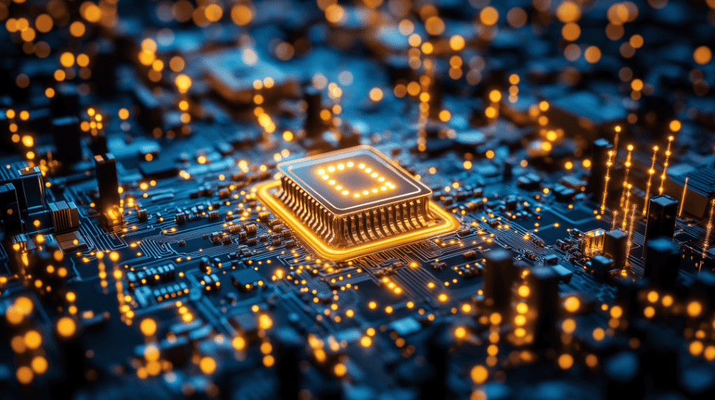
An integrated circuit is a miniature electronic device or component. Using specific processes, the transistors, diodes, resistors, capacitors, inductors, and other components required for a circuit, along with their interconnections, are fabricated together onto a small piece or a few small pieces of semiconductor wafer or dielectric substrate. This structure is then encapsulated within a shell, forming a miniature structure with the desired circuit functions.
All components are structurally integrated into a whole. This significantly reduces the volume of the entire circuit and drastically decreases the number of lead wires and solder joints. Consequently, electronic components have taken a great leap forward in terms of miniaturization, low power consumption, and high reliability.
In circuit diagrams, integrated circuits are represented by the letters “IC” (sometimes the character “N” is also used).
Integrated Circuit Structure Diagram
An integrated circuit is a device that integrates numerous electronic components like transistors, resistors, and capacitors onto a semiconductor chip through complex manufacturing processes. Based on integration density and complexity, integrated circuits can be categorized into several types, including Digital Integrated Circuits, Analog Integrated Circuits, and Mixed-Signal Integrated Circuits.
3 The Historical Evolution of Integrated Circuits
The history of integrated circuits began in 1947 with the invention of the point-contact Ge transistor at Bell Labs. In 1950, Shockley invented the first BJT (Bipolar Junction Transistor). Compared to vacuum diodes, these transistors offered tremendous improvements in reliability, power consumption, and size.
In 1958, Jack Kilby of Texas Instruments invented the first integrated circuit, fabricating two BJTs on germanium, thus initiating the “Silicon Age.” Almost simultaneously, Robert Noyce, who later became the R&D manager at Fairchild Semiconductor, independently proposed the concept of the integrated circuit.
In the 1960s, integrated circuit technology began to develop rapidly. In 1963, Fairchild invented CMOS technology, which used symmetrically complementary NMOS and PMOS devices. Due to its low-power consumption characteristics, CMOS technology eventually became the mainstream technology for integrated circuits.
The 1970s marked a new stage of development with the invention of the microprocessor. In 1971, Intel Corporation introduced the first microprocessor, the 4004. This 4-bit microprocessor was manufactured using P-channel MOS technology, measured 150×110 mils², and integrated approximately 2,300 transistors.
In the 1980s, the model combining fabless IC design companies with standard process foundries began to emerge as a new paradigm for the development of the integrated circuit industry. The world’s first dedicated foundry was Taiwan Semiconductor Manufacturing Company (TSMC), founded in 1987.
During the 1990s, the integrated circuit industry entered an advanced stage oriented towards intense competition, forming a landscape where the design industry, manufacturing industry, packaging industry, and testing industry became independent sectors.
Entering the 21st century, integrated circuit technology continued to develop along Moore’s Law. The most advanced process nodes have now reached the 2-3 nanometer level, with the integration density and performance of integrated circuits continuously improving.
Integrated Circuit Structural Diagram
4 Characteristics and Application Scope of Integrated Circuits
4.1 Characteristics of Integrated Circuits
Integrated circuits offer advantages such as small size, light weight, fewer lead wires and solder joints, long lifespan, high reliability, and good performance, while also being low cost and suitable for large-scale production. They are widely used not only in industrial and civilian electronic equipment like radios, televisions, and computers but also in military, communication, and remote control applications.
Using integrated circuits to assemble electronic equipment can increase the assembly density by tens to thousands of times compared to transistors, and the stable operation time of the equipment can also be significantly improved.
4.2 Application Scope of Integrated Circuits
Integrated circuits are widely used in computing, communications, consumer electronics, automotive electronics, medical equipment, and other fields.
In the consumer electronics sector, a smartphone integrates over 15 ICs, including the AP (Application Processor), BP (Baseband Processor), RF (Radio Frequency Chip), and PMIC (Power Management IC). Wearable devices like the Apple Watch Series 7 use a dual-core S7 chip, integrating a U1 chip and Bluetooth 5.3.
In automotive electronics, autonomous driving systems like the Nvidia DRIVE Thor chip deliver computing power of up to 2000 TOPS. Tesla’s FSD chip integrates a neural network accelerator with a computing power of 144 TOPS.
In industrial control, Siemens’ S7-1500 PLC integrates a PROFINET interface with a scan cycle of <100μs. ABB’s OmniCore controllers achieve synchronous control of 16 axes.
5 Types of Integrated Circuits
Integrated circuits can be classified according to their function, structure, level of integration, and other methods. The following are several main categories:
5.1 Digital Integrated Circuits
Digital integrated circuits are based on binary logic, utilizing the switching characteristics of transistors for information processing. Their development follows Moore’s Law, with integration levels increasing millions of times from early SSI (Small-Scale Integration) to current VLSI (Very-Large-Scale Integration).
Digital integrated circuits include the following typical products:
- Logic Gate Arrays: AND, OR, NOT gates forming the basic units of digital systems.
- Microprocessors: CPU/GPU cores employing superscalar architectures, e.g., the Apple M1 chip integrating 16 billion transistors.
- Memory Devices: DRAM memory bandwidth reaching 6400 MT/s, NAND flash memory stacking layers exceeding 200.
Digital circuit design exhibits three major trends: Heterogeneous Integration combines CPU, GPU, NPU into an SoC; Chiplet Technology enables modular combination; Compute-in-Memory Architecture breaks the von Neumann bottleneck.
5.2 Analog Integrated Circuits
Analog integrated circuits process continuous signals and are irreplaceable in areas such as power management and signal conditioning. Core modules of analog ICs include:
- Operational Amplifiers: Rail-to-rail input, low-noise designs are becoming mainstream.
- Data Converters: ADC sampling rates突破 10 GSPS, with resolutions reaching 24 bits.
- RF Front-Ends: GaN power amplifiers for 5G base stations achieve efficiency exceeding 70%.
A typical application is TI’s TPS61088 power management IC, which achieves 95% conversion efficiency through adaptive on-time control. Analog design faces challenges like process variation and noise coupling, necessitating the use of Top-Down design methodologies.
5.3 Mixed-Signal Integrated Circuits
Mixed-signal chips integrate digital control and analog processing. Typical representatives include:
- ADC/DAC: JESD204B interface enables high-speed data transfer.
- Phase-Locked Loops (PLL): Sub-picosecond jitter meets SerDes clock requirements.
- Sensor Interfaces: Integrated biosignal sensors enable μV-level signal detection.
A key design difficulty is the interference caused by substrate noise from the digital sections on the analog circuits, requiring techniques like guard ring isolation and independent power domains.
Table: Integrated Circuits Classified by Integration Level
| Integration Level | Number of Transistors | Representative Circuits |
|---|---|---|
| Small-Scale Integration (SSI) | 10-100 | Logic Gates, Flip-Flops |
| Medium-Scale Integration (MSI) | 100-1,000 | Encoders, Decoders |
| Large-Scale Integration (LSI) | 1,000-10,000 | 8-bit Microprocessors, Memory |
| Very-Large-Scale Integration (VLSI) | 10^4-10^6 | 16/32-bit Microprocessors |
| Ultra-Large-Scale Integration (ULSI) | 10^6-10^9 | 64-bit Microprocessors, SoCs |
| Giga-Scale Integration (GSI) | >10^9 | High-Performance CPUs, GPUs |
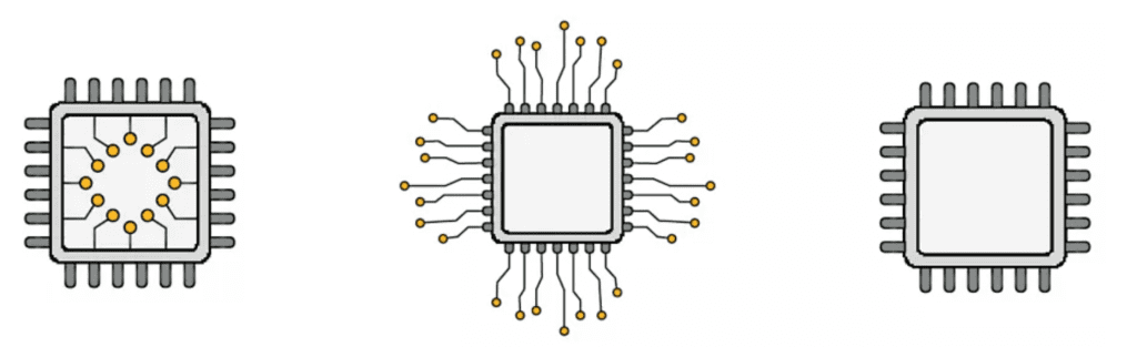
6 Integrated Circuit Package Types
Integrated circuit packaging is the external structure that protects and connects the chip. It not only provides mechanical protection and a thermal path but also enables electrical connections between the chip and the external circuit. Common integrated circuit package types include:
6.1 Classification by Shape
Based on physical characteristics, IC packages can be divided into these main types:
- Circular Package: Metal can transistor package type, generally suitable for high-power devices.
- Flat Type: Good stability, small size.
- Dual In-line Package (DIP): The main package form for early microcircuits, typically with a pin pitch of 2.54mm.
6.2 Classification by Packaging Material
Depending on the material used, IC packages can be categorized as:
- Metal Packaging: Offers good heat dissipation and electromagnetic shielding, often used in high-reliability fields.
- Ceramic Packaging: Provides excellent thermal stability and hermeticity, suitable for military, aerospace, and other demanding applications.
- Plastic Packaging: Low cost, mature process, currently the most common packaging form for commercial integrated circuits.
6.3 Classification by Pin Layout
Based on pin arrangement, IC packages can be divided into:
- Through-Hole Mounting (THM): e.g., DIP (Dual In-line Package), PGA (Pin Grid Array).
- Surface-Mount Technology (SMT): e.g., SOP (Small Outline Package), QFP (Quad Flat Package), BGA (Ball Grid Array).
As integrated circuit technology advances, packaging technology also continuously evolves, moving towards miniaturization, higher density, and improved performance.
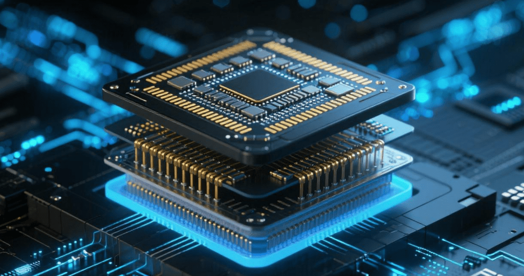
7 What are 2.5D and 3D Integrated Circuits?
As Moore’s Law gradually approaches its physical limits, traditional two-dimensional planar integration faces challenges. 2.5D and 3D integrated circuit technologies have emerged as important pathways for continuing the performance enhancement of integrated circuits.
7.1 2.5D Integrated Circuits
2.5D integration is a transitional technology between traditional 2D and full 3D integration. In 2.5D integration, multiple chips are placed side-by-side on a silicon interposer. Communication between chips occurs through high-density interconnects on the interposer, which is then connected to the package substrate via solder balls.
A typical representative of 2.5D integration technology is TSMC’s CoWoS (Chip-on-Wafer-on-Substrate) technology, which enables the 3D stacking of HBM3 memory with GPUs, achieving bandwidths up to 3 TB/s.
The main advantages of 2.5D integration include:
- Enables high-density interconnects, far exceeding the density of traditional packaging.
- Ability to integrate chips manufactured using different process nodes.
- Easier thermal management compared to 3D integration.
- High design flexibility, allowing for optimized system performance.
7.2 3D Integrated Circuits
3D integrated circuits stack chips vertically and use Through-Silicon Vias (TSVs) for inter-layer connections. 3D integration enables shorter interconnect lengths, higher integration density, and better performance.
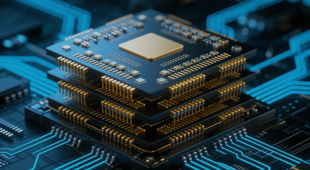
Intel’s Foveros technology enables vertical interconnection between logic chips and SRAM, achieving an interconnect density of 10,000 connections/mm².
The main advantages of 3D integrated circuits include:
- Reduced interconnect length, lowering signal delay and power consumption.
- Greatly increased integration density, packing more functionality into a limited area.
- Strong heterogeneous integration capability, allowing the integration of chips from different processes and materials.
- Enhanced system performance due to shortened interconnects.
7.3 Comparison of 2.5D and 3D Integration
Table: Comparison of 2.5D and 3D Integrated Circuit Technologies
| Characteristic | 2.5D Integration | 3D Integration |
|---|---|---|
| Interconnect Method | Horizontal via Silicon Interposer | Vertical via TSVs |
| Interconnect Density | High | Very High |
| Thermal Management | Relatively Easier | Major Challenge |
| Process Complexity | Relatively High | High |
| Cost | High | High |
| System Performance | Significant Improvement | Notable Improvement |
| Representative Technology | TSMC’s CoWoS | Intel’s Foveros |
8 Summary
As the cornerstone of modern electronic technology, the development of integrated circuits has profoundly influenced technological progress in human society. Since Jack Kilby invented the first integrated circuit in 1958, this field has experienced a leapfrog development from simplicity to complexity, and from single functions to system integration.
The global integrated circuit market has now reached a scale of trillions of dollars. China, as the largest consumer, accounts for 25% of the global market share. Driven by emerging applications like AI, 5G, and new energy vehicles, integrated circuits are evolving towards heterogeneous integration, 3D stacking, and new material applications.
The future development trend of integrated circuit technology is towards miniaturization, higher speed, and energy efficiency. Research into new materials, 3D integration, and quantum technologies is becoming increasingly active. As the world’s largest market, China has formed a competitive advantage in the packaging and testing环节, but still needs breakthroughs in areas like EDA tools and advanced process nodes.
Over the next decade, integrated circuit technology will continue to drive the digital economy, remaining a core element of national scientific and technological competitiveness.


0 Comments