
Introduction
As computer technology and electronic products have permeated almost every aspect of our lives, it’s easy to overlook or ignore the very foundation upon which they are built: the Printed Circuit Board (PCB). Despite the ubiquity of electronics and their components in our daily lives, they have emerged only within the last century or so. The Printed Circuit Boards (PCBs) used in modern electronic devices were first designed and developed in the 1930s.
In 1936, Austrian inventor Paul Eisler, building upon circuit designs initially patented by Charles Ducas, developed the first printed circuit board (PCB) for operating a radio system. This technology was quickly adopted by the US military and used in proximity fuses during World War II. Released to the public in 1948, the printed circuit board—also known as a Printed Wiring Board (PWB)—began its evolution.
To help you understand the history of the PCB, we have provided a timeline outlining the major discoveries, changes, and breakthroughs that have shaped the PCB into what it is today.
PCBs in the Modern Era
A printed circuit board is a component inside electronic devices that transmits electrical signals. Whenever you turn on a computer or press a button on a smartphone, radio alarm clock, or stereo, you are interacting with a printed circuit board located inside the casing of all these devices. If electricity is the lifeblood of electronics, then the printed circuit board is the vital internal organ.
In today’s highly device-dependent world, most people are scarcely aware that every smartphone or portable MP3 player contains complex circuitry. Modern technology would be impossible without printed circuit boards.
Today, printed circuit boards are no longer mistakenly identified with chemical PCBs but are openly referred to as PCBs without confusion. This is largely due to the gradual phasing out of chemical PCBs over the past four decades. The terms Printed Circuit Board and Printed Wiring Board (PWB) are now used interchangeably within the industry, though Printed Circuit Board is more commonly used today.
As printed circuit boards continue to evolve, they are expected to become smaller in size and more complex in structure. A recent innovation in PCB technology—the rigid-flex PCB—combines the complexity and reliability of rigid board circuits with flexible layers integrated into the rigid structure. With these flexible layers, rigid-flex PCBs become smaller, thinner, and capable of adapting to uniquely shaped or extremely small products.
What is a Printed Circuit Board?
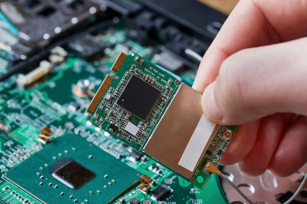
A Printed Circuit Board (PCB) is a substrate device etched with electronic components. PCBs can be single-sided, double-sided, or multi-layer, with corresponding copper layers. The highest density PCBs consist of multiple layers. These PCBs contain plated-through holes used to connect conductors on different layers. In more complex PCBs, the substrate often incorporates laminated capacitors, resistors, and other components. The layers of most rigid PCBs are typically composed of a substrate made from FR-4 glass epoxy.
PCBs are indispensable in almost all electronic devices except the simplest products. PCB design involves complex circuit details, but their assembly and production can be standardized. Because PCBs are assembled from pre-fabricated and wired components, their mass production process is straightforward, relatively low-cost, and typically error-free, especially when compared to other wiring methods like point-to-point and wire wrap.
The abbreviation PCB applies to both bare boards and assembled boards. If a board has copper connections but lacks embedded components, the more appropriate term would be Printed Wiring Board, although this term has largely fallen out of technical use. Other more common terms include Printed Circuit Board Assembly and Printed Circuit Assembly, the latter referring to a PCB with electronic components mounted on it.
The development history of PCBs is essentially a history of the evolution of the electronics industry. From simple circuits in early radios to the complex multi-layer boards that now support artificial intelligence and 5G communications, every leap in PCB technology has profoundly influenced the form and function of electronic products. Below is a detailed, chronological overview of the complete development journey of the PCB.
Overview of PCB Development History
| Era/Stage | Key Characteristics | Major Breakthroughs & Representative Events |
|---|---|---|
| Early 1900s-1940s (Origins & Prototype) | Conceptual shift from “wire harness connections” to “printed circuits”; exploration of fundamental manufacturing processes. | 1903: Albert Hanson proposed a concept similar to through-hole boards; 1927: Charles Ducas invented the “printed wiring” technique; 1941: Paul Eisler manufactured the first functional PCB for use in a radio. |
| 1950s-1970s (Technological Development & Scalability) | Industrial mass production of PCBs realized; transition from single-sided to double-sided and multi-layer boards; rapid progress in design and manufacturing technologies. | Early 1950s: Copper foil etching became mainstream, enabling industrial production of single-sided boards; 1960s: Breakthrough in hole metallization enabled mass production of double-sided boards; 1970s: Rapid development of multi-layer boards and the initial adoption of Surface Mount Technology (SMT). |
| 1980s-1990s (Electronics Proliferation & Globalization) | SMT became the mainstream; industry focus shifted to Asia; China emerged as a major production base. | 1980s: Surface Mount Technology (SMT) boards gradually became the production standard; 1990s: The PCB industry began shifting to China and other Asian regions; domestic Chinese industry level rose rapidly through foreign investment and technology introduction. |
| 21st Century Onwards (High-Performance & Diversified Development) | Driven by new demands from mobile internet, AI, and 5G, HDI, flexible boards, high-frequency/high-speed boards, and ultra-high-layer-count boards became technological focal points. | Widespread application of Flexible Printed Circuits (FPC) and high-frequency/high-speed boards; 2025: OKI Circuit Technology introduced a 124-layer PCB, breaking the previous industry ceiling of 108 layers; emergence of advanced packaging technologies like embedded chips and copper posts. |
Detailed Development Stages
Early 1900s-1940s: Origins and Prototype
Before the invention of the PCB, internal connections in electronic devices relied on complex, bulky, and fragile wire harnesses. This connection method was not only time-consuming and costly to manufacture but also highly unreliable. In the early 20th century, engineers began seeking more efficient and compact connection solutions, and the concept of the PCB emerged in this context.
Key advancements during this stage were primarily focused on exploring basic processes. In 1903, German inventor Albert Hansen proposed a prototype similar to modern through-hole boards by attaching wires to an insulating board and creating through-holes for double-sided conduction. In 1927, French inventor Charles Ducas used conductive ink to print circuits on an insulating substrate and patented this process as “printed wiring,” which is considered an early form of modern electroplating.
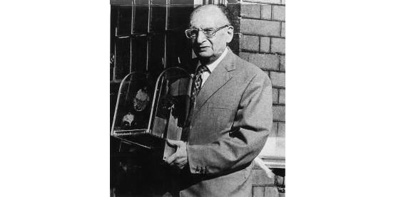
The first working PCB was actually manufactured by Austrian engineer Paul Eisler. In 1941, he used copper foil adhered to an insulating board to create conductive paths, closely resembling the modern PCB. In 1943, he applied this technology in a radio. Coinciding with World War II, PCBs began to be used in military equipment due to their compactness and reliability,初步 demonstrating their technical value.
Although these early inventors laid the groundwork, PCB manufacturing at the time still relied on manual operations, with crude processes and low efficiency. Nonetheless, this groundbreaking creation from scratch sowed the most important seeds for the future revolution in electronic technology.
1950s-1970s: Technological Development and Scalability
After World War II, with the emergence of complex electronic devices like vacuum tube computers, the need for standardized and scalable PCB production became urgent. The previous manual methods could no longer meet demand. The introduction of chemical etching technology became a key breakthrough, using chemical methods to etch fine circuits onto insulating boards, significantly improving production efficiency and precision.
In the early 1950s, issues with the bond strength between the copper foil of Copper Clad Laminates (CCL) and the laminate itself, as well as solder resistance, were resolved, leading to stable and reliable performance. This marked PCB’s entry into the stage of industrial mass production, with single-sided boards becoming mainstream. By the 1960s, a breakthrough in hole metallization technology was achieved. This enabled electrical interconnection between different layers of the board, thereby driving the mass production of double-sided boards.
Entering the 1970s, electronic equipment functions became increasingly complex, and Integrated Circuits (ICs) began to be widely used. ICs significantly reduced the size of electronic components, requiring PCBs to support denser circuits within a smaller area. To meet this challenge, multi-layer board technology developed rapidly, using microvia technology to connect circuits on different layers, achieving higher density wiring. Simultaneously, Surface Mount Technology (SMT) began to gain popularity. Components could now be mounted directly onto the PCB surface, further enhancing assembly efficiency, circuit reliability, and integration compared to traditional through-hole mounting.
During this period, the design and manufacture of PCBs began to form a standardized industrial system, establishing preliminary standards for materials, processes, and design specifications, paving the way for the subsequent miniaturization and increased complexity of electronic devices.
1980s-1990s: Electronics Proliferation and Globalization
Starting in the 1980s, personal computers, home appliances, and early mobile communication devices began to proliferate globally. Electronics entered the consumer market, placing higher demands on PCB output, cost, and reliability. Surface Mount Technology (SMT) gradually completely replaced through-hole technology during this period, becoming the mainstream PCB production method. SMT not only reduced component size and increased assembly automation but also laid the foundation for later developments in high-density packaging technology.
The 1990s was a period of deepening global division of labor, and the PCB industry underwent a significant geographical shift. Due to its low production costs and huge market potential, China attracted substantial investment from PCB manufacturers in Hong Kong, Taiwan, and Japan. This influx, combined with the efforts of domestic Chinese companies, enabled China’s PCB industry to advance by leaps and bounds within just a few years, gradually moving from primarily producing low-layer-count single and double-sided boards towards high-layer-count boards and package substrates in the high-end sector.
Simultaneously, the evolution of chip packaging technology was also driving PCB upgrades. Starting in the 1990s, surface mount technology evolved further from Quad Flat Package (QFP) to Ball Grid Array (BGA) packaging, which placed more stringent demands on PCB wiring density and reliability. At the turn of the millennium in 2000, approximately 70% of global PCB production value was still concentrated in North America, Europe, and Japan. However, by 2003, China’s PCB output value had surpassed that of the United States, becoming the world’s second-largest PCB producer. In 2006, it successfully overtook Japan to become the global leader. This shift fundamentally altered the competitive landscape of the global PCB industry.
21st Century Onwards: High-Performance and Diversified Development
Entering the 21st century, the explosive growth of mobile devices like smartphones and tablets placed extreme demands on PCBs for thinness, lightness, and high performance. To adapt to the limited space inside devices, Flexible Printed Circuits (FPC) were widely adopted. They can bend and fold, enabling complex routing in three-dimensional space. Furthermore, the rise of applications like 5G communication and data centers required fast signal transmission speeds with low loss, driving the continuous development of high-frequency and high-speed PCB technology.
Emerging fields such as Artificial Intelligence (AI), the Internet of Things (IoT), and new energy vehicles became new engines driving PCB technology forward at a rapid pace. To meet the testing and interconnection needs of advanced chips like High Bandwidth Memory (HBM) in AI servers, the layer count of PCBs was pushed to new heights. For example, the 124-layer PCB launched by OKI Circuit Technology in 2025 broke the long-standing industry ceiling of 108 layers within a standard board thickness, achieving unprecedented signal density and vertical interconnection.
Another notable trend is the integration of advanced packaging and PCBs. For instance, the “Copper Post (Cu-Post) Technology” introduced by LG Innotek replaces some traditional solder balls with copper posts to connect chips and substrates, achieving a 20% reduction in connection pitch and a several-fold improvement in heat dissipation efficiency. Additionally, embedded component technology directly embeds components like chips and inductors within the PCB substrate itself, representing a paradigm shift from two-dimensional circuits to three-dimensional system integration, significantly enhancing system integration density and performance.
Current Status and Future Outlook
Current Status
Today, PCBs have become the cornerstone of the global electronics industry, with their output value continuously growing. According to industry data, the global PCB industry output value is projected to reach $86.33 billion in 2025. The current industry landscape is characterized by the following:
- Concentrated Technological Focus: Industry innovation is primarily concentrated on meeting the demands of high-end applications like AI, 5G, and automotive electronics. High-layer-count boards, HDI (High-Density Interconnect), flexible boards, and IC substrates are the key focuses of R&D and investment.
- Collaborative Supply Chain Innovation: To overcome cutting-edge technological challenges, collaboration between upstream and downstream companies in the supply chain is becoming increasingly close. For example, the “national team” model, comprising network equipment providers, PCB manufacturers, material suppliers, and research institutions, formed to break through 3.2T ultra-high-speed network connector technology, demonstrates the advantage of collaborative efforts.
- Evolving Competitive Landscape: The explosive demand for AI has spawned a high-end PCB market specifically for AI servers, attracting numerous leading manufacturers to enter this segment. Analysis suggests that despite the gradual increase in production capacity in the short term, the AI PCB market is expected to maintain a healthy supply-demand balance at least until 2027.
Future Trends
Looking ahead, the development of PCB technology will be deeply intertwined with emerging electronic application scenarios, presenting the following trends:
- Continuous Performance Enhancement and Integration: The pursuit of higher computational speeds and data throughput is relentless. Novel architectures like orthogonal backplanes, along with PCB materials and stack-up technologies for next-generation ultra-high-speed networks (e.g., 3.2T), will be key future breakthroughs. Simultaneously, 3D integration technologies that embed passive and even active chips within the board will continue to blur the line between PCBs and packaging, achieving higher system performance.
- Innovation in Materials and Processes: Underlying material innovation is fundamental to PCB advancement. Extremely Low Loss (ELL) substrate materials, metal substrates with better thermal conductivity, and dielectric materials suitable for higher frequencies will be R&D priorities. In manufacturing processes, additive manufacturing (3D printing) and AI-driven EDA design tools are expected to enhance design freedom and optimize production yield.
- Deepening and Broadening Application Scenarios: PCBs will find broader application space in the “Internet of Everything” intelligent world. From cloud data centers to edge AIoT devices, and further to sensors and control systems in smart automobiles, the PCB, as a bridge connecting the physical world with digital information, will see its importance increasingly highlighted.
Summary and Recommendations
Reflecting on the over-century-long development history of PCBs, they have evolved from a simple connection technology into a key component determining the performance of electronic products. For those interested in this field, whether for investment, career choices, or technical learning, the following directions are worth focusing on:
- Track Cutting-Edge Technologies: Pay close attention to the latest advancements in PCB-related technologies such as AI servers, high-speed connectors, and advanced packaging (e.g., embedded chips, copper post technology).
- Understand Market Dynamics: Comprehend the specific driving effects of mainstream applications like 5G, IoT, new energy vehicles, and artificial intelligence on PCB demand.
- Monitor Industry Chain Dynamics: The development of PCBs is inseparable from upstream and downstream collaboration. Therefore, it is also necessary to maintain an understanding of key material sectors such as copper-clad laminates, specialty resins, and electronic fiberglass cloth, as well as core equipment areas like etching, electroplating, and vacuum lamination.
We hope this detailed summary of the history of PCB development helps you better understand this crucial cornerstone of the electronics industry. If you have a deeper interest in a specific technical area or application scenario, we would be pleased to continue the discussion.


0 Comments