
Introduction
In modern electronic systems, the importance of Power Management Technology is self-evident, as it directly affects the performance, energy efficiency, and reliability of electronic equipment. Buck regulators, as a core component of power management integrated circuits, efficiently convert a higher input voltage to a lower, stable output voltage, meeting the broad needs ranging from portable devices to industrial systems. According to market research statistics, the global revenue of buck-boost switching regulators reached approximately 683 million RMB in 2024 and is projected to grow to 1.16 billion RMB by 2031, representing a Compound Annual Growth Rate (CAGR) of 7.8%. This significant growth trend fully reflects the increasing demand for efficient, miniaturized power solutions in electronic devices.
The booming market for buck regulators is driven by various technical factors. On one hand, the continuous improvement in the functional integration of electronic devices imposes higher requirements on power management, necessitating more precise voltage rail management and higher conversion efficiency. On the other hand, the rapid development of IoT devices and automotive electronics has created new application scenarios for buck regulators. Particularly in automotive electronics, with the proliferation of Advanced Driver-Assistance Systems (ADAS), in-vehicle infotainment systems, and electric powertrains, the demand for high-reliability, high-efficiency buck regulators has surged. The market size for high-voltage buck regulator ICs (greater than 60V) reached $624 million in 2024 and is expected to reach $952 million by 2031.
This article will delve into the core technical characteristics, application fields, and performance parameters of buck regulators, providing professional reference for electronic engineers in selecting and designing power management systems. Through a comprehensive analysis of the working principles, design considerations, and development trends of buck regulators, we can better grasp the important position and future potential of this key component in modern electronic systems.
What is a Buck Regulator?
A buck regulator, also known as a buck converter, is a DC-DC converter capable of converting an input voltage to a lower, stable output voltage. Unlike linear regulators, buck regulators employ switching technology, utilizing high-speed switching elements and energy storage components (inductors, capacitors) to achieve efficient power conversion. Their core function is to maintain a constant output voltage regardless of variations in input voltage or load current, providing stable and reliable power for various integrated circuits within electronic systems.
From a circuit structure perspective, a buck regulator primarily consists of a power switch (typically a MOSFET), a diode or synchronous rectification switch, an inductor, and an output capacitor. The switch turns on and off alternately at a fixed frequency (typically from tens of kHz to several MHz), regulating the output voltage by controlling the duty cycle of the on-time. When the switch is on, the input power supplies the inductor and load, storing energy in the inductor. When the switch is off, the inductor releases the stored energy, continuing to supply the load through the freewheeling path. Through this alternating process, the output voltage is precisely controlled at the set value.
Compared to linear regulators, buck regulators have a distinct advantage in terms of efficiency. Linear regulators stabilize the output voltage by dissipating excess power, with efficiency approximately equal to the ratio of output voltage to input voltage. This efficiency drops significantly when the input-output voltage difference is large. In contrast, buck regulators achieve energy conversion through switching operation, typically achieving efficiencies of 85%-95% or even higher, largely unaffected by a large input-output voltage difference. This characteristic makes buck regulators particularly suitable for applications with wide input voltage variations or large input-output voltage differentials.

Compared to Low-Dropout Regulators (LDOs), each has its suitable scenarios. LDOs offer advantages of low noise, fast response, and simple structure, making them particularly suitable for applications with small input-output voltage differences and high noise sensitivity, such as RF circuits and analog sensors. However, LDOs suffer from low efficiency under high dropout conditions and are only suitable for low-current applications. Buck regulators are suitable for applications requiring higher current and high efficiency, such as processor core power supplies and motor drives, at the cost of more complex design and potential switching noise.
Table: Comparison of Different Types of Regulators
| Characteristic | Buck Switching Regulator | Linear Regulator | Low-Dropout Regulator (LDO) |
|---|---|---|---|
| Conversion Efficiency | High (85%-95%) | Low (~Vout/Vin) | Medium (Depends on Dropout) |
| Power Density | High | Low | Medium |
| Noise Level | High (Switching Noise) | Low | Very Low |
| Complexity | High | Low | Low |
| Cost | Medium-High | Low | Low |
| Suitable Current | High Current (Multi-phase up to tens of Amps) | Low Current (<1A) | Low to Medium Current (<3A) |
Basic Theory and Equations of Buck Converters
The fundamental operating principle of a buck converter is based on Pulse Width Modulation (PWM) technology, regulating the output voltage by controlling the proportion of on-time of the switching element. During a complete switching cycle, when the high-side switch is on, the input voltage is applied across the inductor and load, causing the inductor current to increase linearly and storing energy in the magnetic field. When the high-side switch is off, the inductor current continues to flow through the low-side switch or freewheeling diode, decreasing linearly as the stored energy is released to the load. Through this periodic process of storing and releasing energy, the output voltage is stabilized at the preset value.
The fundamental equation describing the behavior of a buck converter is based on the volt-second balance principle, which states that the integral of the voltage across the inductor over a complete switching cycle must be zero to maintain flux balance. This principle leads to the core equation of the buck converter:
Vout = D × Vin
Where D is the duty cycle of the switch, defined as the ratio of on-time to the switching period (D = Ton / T). This equation indicates that the output voltage of the buck converter equals the input voltage multiplied by the duty cycle, allowing precise control of the output voltage by adjusting D. For example, with an input voltage of 12V and a required output of 3.3V, the required duty cycle is approximately 27.5%.
In practical design, inductor selection is crucial for converter performance. The inductor value determines the magnitude of the ripple current, the peak-to-peak fluctuation of the inductor current during the switching cycle. The ripple current ΔIL is calculated as:
ΔIL = (Vin – Vout) × D / (fsw × L)
Where fsw is the switching frequency and L is the inductance value. A larger inductor value reduces the ripple current but can slow down the transient response and increase physical size. A smaller inductor results in larger ripple current and might cause the converter to enter Discontinuous Conduction Mode (DCM). Typically, the ripple current is recommended to be 20%-40% of the maximum output current to balance size and performance.
The output capacitor influences the output voltage ripple. During switching operation, the output capacitor supplies high-frequency current demanded by the load and suppresses voltage fluctuations. The output voltage ripple ΔVout is primarily determined by the capacitor’s Equivalent Series Resistance (ESR) and its capacitance value:
ΔVout = ΔIL × (ESR + 1 / (8 × fsw × Cout))
To achieve low output voltage ripple, capacitors with low ESR, such as ceramic or low-ESR polymer capacitors, should be selected. For instance, the TLV775 LDO regulator recommends using an output capacitor between 0.47μF and 40μF, with an ESR less than 100mΩ.
Buck converters have two basic operating modes: Continuous Conduction Mode (CCM) and Discontinuous Conduction Mode (DCM). In CCM, the inductor current always remains greater than zero throughout the entire switching cycle, suitable for higher load currents. In DCM, the inductor current falls to zero for a portion of each switching cycle, common under light load conditions. The voltage conversion relationship in DCM is more complex, and ripple current is higher, but it can reduce switching losses under light loads.
Modern buck regulator ICs typically employ voltage-mode control or current-mode control. Voltage-mode control adjusts the duty cycle based solely on the output voltage error; it is simple but has slower transient response. Current-mode control monitors both the inductor current and output voltage, providing faster transient response and inherent overcurrent protection, making it a mainstream solution. Furthermore, some advanced buck controllers incorporate Constant On-Time (COT) control, offering optimal transient response under varying input and output conditions.
Components of a Buck Regulator
The performance and reliability of a buck regulator depend heavily on the selection and configuration of its individual components. A typical buck regulator comprises several key components, each playing a unique and vital role in the system. A deep understanding of these components and their interactions is essential for optimizing buck regulator design.
The Power Switch is the core component of the buck regulator, responsible for rapidly switching the current path. Modern buck regulators typically use MOSFETs as power switches due to their advantages of simple drive requirements, fast switching speed, and low on-resistance. Power switches can be divided into the high-side (control) switch and the low-side (synchronous) switch; in non-synchronous rectification designs, the low-side switch is replaced by a diode. For example, STMicroelectronics’ DCP0606Y integrates both high-side and low-side MOSFETs, reducing the number of external components. Selecting a power switch involves balancing parameters like on-resistance (Rds(on)), gate charge, switching speed, and voltage rating to optimize efficiency and cost.
The Inductor is the energy storage element in the buck converter, smoothing the pulsed current generated by the switch. During the switch on-time, the inductor stores energy, and its current increases linearly. During the switch off-time, the inductor releases energy, and its current decreases linearly. The inductor value determines the ripple current magnitude and is typically selected based on switching frequency, input/output voltages, and the desired ripple current. For instance, in a 2MHz buck converter, inductor values usually range from 1μH to 4.7μH. Additionally, the inductor should have low DC resistance to minimize conduction losses and a sufficient saturation current rating to prevent core saturation.
The Output Capacitor maintains a stable output voltage and filters the voltage ripple caused by switching. When the inductor current exceeds the load current, the capacitor charges; when the inductor current is less than the load current, the capacitor discharges, thereby smoothing the output voltage. Selecting the output capacitor involves considering capacitance value, Equivalent Series Resistance (ESR), and rated voltage. As mentioned, the TLV775 LDO recommends an output capacitor between 0.47μF and 40μF with ESR < 100mΩ. Low-ESR capacitors like ceramics or polymers significantly reduce output voltage ripple. The Equivalent Series Inductance (ESL) also affects high-frequency performance, especially in applications with MHz-range switching frequencies.
The Input Capacitor is located at the input of the buck regulator, providing local energy buffering for the switching operation and reducing current surges drawn from the input source. When the high-side switch turns on, the instantaneous high current is primarily supplied by the input capacitor rather than directly from the input source. The input capacitor needs low ESR and ESL to effectively filter switching noise. TI’s TLV775 datasheet recommends using a 1μF input capacitor to counteract source resistance and inductance. In practice, multiple capacitors of different values are often paralleled to provide a low-impedance path over a wide frequency range.
The Control IC is the brain of the modern buck regulator, integrating functions such as the PWM controller, error amplifier, protection circuits, and driver circuits. The control IC monitors the output voltage, compares it to a reference voltage, and adjusts the switch duty cycle based on the error to maintain a stable output. Advanced control ICs offer additional features like enable control, power-good indicators, soft-start, and frequency synchronization. The DCP0606Y, for example, integrates control logic, protection circuits, and soft-start functionality, allowing the switching frequency to be set via a single resistor. The performance of the control IC directly determines the regulator’s voltage accuracy, transient response, and reliability.
The Feedback Network, typically a resistor divider, scales down the output voltage to a level comparable to the control IC’s reference voltage. The ratio of the feedback resistors sets the output voltage value according to Vout = Vref × (1 + R1/R2). To minimize power consumption and improve accuracy, larger resistor values are usually chosen, though excessively high values can increase noise sensitivity. Some designs also add compensation networks to the feedback loop to improve stability.
Protection Circuits are key to ensuring the reliable operation of the buck regulator and commonly include overcurrent protection (OCP), overvoltage protection (OVP), undervoltage lockout (UVLO), and thermal shutdown (OTP). These functions are now often integrated into the control IC. The DCP0606Y includes overvoltage, overcurrent, and overtemperature protection mechanisms with auto-recovery capability. OCP prevents damage from output shorts or overloads; OVP protects the load in case of feedback loop failure; UVLO ensures the regulator remains off when input voltage is insufficient; and OTP shuts down the regulator if the chip temperature becomes excessive.
In practical design, the selection of these components requires a comprehensive consideration of performance, size, cost, and reliability requirements. For example, portable devices prioritize high efficiency and small size; industrial applications focus more on reliability and temperature range; automotive electronics must meet stringent reliability standards and temperature requirements. Reasonable selection and configuration of these components are essential for optimizing the overall performance of the buck regulator.
Main Characteristics of Buck Regulators
1. High Efficiency
Buck regulators are renowned for their high efficiency, often exceeding 90%. This efficiency is achieved because the regulator converts excess voltage into useful output power rather than dissipating it as heat, as linear regulators do. Linear regulators directly dissipate excess voltage, wasting power and generating heat. Buck regulators transfer power through a switching mechanism, minimizing energy loss and heat generation.
This high efficiency is particularly important for battery-powered devices like smartphones, laptops, and wearables, as energy savings directly translate to extended battery life. For example, using a linear regulator to drop voltage from 12V to 5V would waste over 50% of the power, whereas a buck converter performing the same operation wastes only 5-10% of the power. In high-power applications like server farms, this high efficiency reduces the need for extensive cooling solutions and extends component lifespan by lowering thermal stress.
2. High Switching Frequency
Buck regulators operate at high switching frequencies, typically ranging from hundreds of kilohertz (kHz) to several megahertz (MHz). The advantage of a high switching frequency is that it allows the use of smaller passive components, such as inductors and capacitors. Smaller components enable more compact circuit designs, which is crucial for modern electronics with limited space, like smartphones, tablets, and wearables.
While higher switching frequencies reduce the size of these components, they also lead to increased switching losses. Therefore, engineers must find a balance between frequency and efficiency based on application requirements. High frequencies enable more compact designs but require careful consideration to avoid unnecessary efficiency losses.
3. Wide Input Voltage Range
Buck regulators are versatile, capable of handling a wide input voltage range, often from 3V to 40V or more, allowing them to adapt to various power supply configurations. This flexibility is crucial in applications like automotive or industrial systems where input voltage can vary significantly. For example, a buck regulator can step down a high supply voltage like 24V to the lower voltage required by the load (e.g., 3.3V or 5V).
In automotive systems, where battery voltage can fluctuate due to engine cranking or load changes, this wide input range ensures the buck regulator maintains a stable output voltage. The ability to adapt to different input levels enhances the regulator’s versatility and reduces the need for different designs for each specific system.
4. Continuous and Discontinuous Modes
Buck regulators can operate in either Continuous Conduction Mode (CCM) or Discontinuous Conduction Mode (DCM), depending on the load current. In CCM, the current through the inductor never falls to zero, resulting in smoother operation and lower output ripple. This mode is more common under heavier loads. DCM occurs under lighter loads, where the inductor current drops to zero for a portion of the switching cycle, potentially improving efficiency but possibly increasing output ripple.
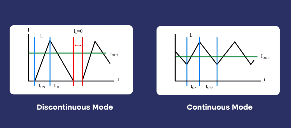
Switching between these modes allows the regulator to optimize performance under different load conditions. Under light loads, DCM can reduce switching losses and improve efficiency, while under heavy loads, CCM maintains stable, low-ripple output. Modern regulators often automatically switch between these modes to ensure an optimal balance of efficiency and performance.
5. Synchronous vs. Non-Synchronous Design
Synchronous buck regulators replace the conventional diode with a MOSFET that is actively controlled to reduce power loss. This improvement is particularly important in low-voltage applications because even a small voltage drop across a diode can significantly impact efficiency. A typical diode has a forward voltage drop of around 0.7V, which can be substantial when the output voltage is low (e.g., 1.8V or 1.2V).
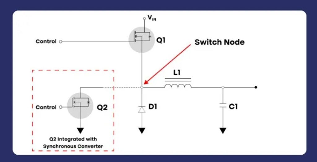
Synchronous buck regulators minimize these losses by using a low-Rds(on) MOSFET instead of a diode, improving efficiency by 2-5% in many cases. This design is especially beneficial for applications where power efficiency is critical, such as in processors and other electronics with tight power budgets.
6. Low Output Voltage Ripple
Buck regulators are designed to minimize output voltage ripple – the small residual AC voltage present on the DC output. Ripple can affect sensitive circuits, causing errors or noise in analog and digital systems. Buck regulators achieve low ripple through the use of output capacitors and precise control of the switching cycle.
[Image: Output Waveform – Placeholder for diagram showing the output voltage waveform with ripple superimposed on the DC level.]
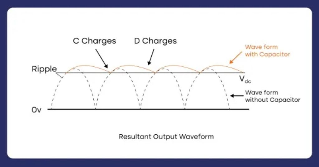
Low ripple is especially important in devices where signal integrity is critical, such as audio equipment, precision analog circuits, and communication systems. For instance, microcontrollers and RF circuits might malfunction or exhibit degraded performance if exposed to high ripple, making ripple suppression an important aspect of buck regulator design.
Applications of Buck Regulators
Buck regulators, known for their efficiency, flexibility, and reliability, have become critical power management solutions across numerous fields. From portable consumer electronics to harsh automotive environments, and from low-power to high-power applications, buck regulators play an indispensable role.
Consumer Electronics is one of the largest application areas for buck regulators. Portable electronic products like smartphones, tablets, and wearable devices widely use buck regulators to provide multiple voltage rails for processors, memory, displays, and RF circuits. In these applications, high efficiency and small size are primary considerations, directly impacting device battery life and physical size. For instance, smartphones often integrate multiple buck regulators, forming multi-phase power architectures to supply core voltage for high-performance application processors, with current capabilities reaching several amps or even tens of amps. Wearable devices place greater emphasis on light-load efficiency to extend battery life. The switching frequency of buck regulators in consumer electronics is typically high (above 1MHz) to allow the use of smaller inductors and capacitors, meeting the demands for thin, light, and small designs.
Automotive Electronics is experiencing rapidly growing demand for buck regulators, especially with the proliferation of electric vehicles, Advanced Driver-Assistance Systems (ADAS), and in-vehicle infotainment systems. The automotive environment imposes extremely stringent requirements on electronic components, including wide temperature ranges, high reliability, and immunity to voltage transients and electromagnetic interference. For example, STMicroelectronics’ DCP0606Y is designed specifically for automotive applications, providing up to 6A of output current with a minimum output voltage as low as 0.6V. It is suitable for automotive telematics systems, head-up displays, infotainment systems, camera digital core power, and ADAS. Automotive buck regulators typically require AEC-Q100 qualification to ensure reliable operation within a temperature range of -40°C to 150°C.
Industrial Applications cover fields such as factory automation, process control, test and measurement, and industrial robotics, which place extremely high demands on the reliability and robustness of buck regulators. Power sources in industrial environments are often noisy and subject to surges and transients, so industrial-grade buck regulators need higher noise immunity and wider operating temperature ranges. High-voltage buck regulator ICs (greater than 60V) are widely used in industrial power supplies, with a market size of $624 million in 2024. Industrial buck regulators typically need to support wide input voltage ranges, such as 4.5V to 60V or wider, to adapt to 24V industrial buses and battery-powered systems. Furthermore, buck regulators in industrial applications must meet safety standards and reliability requirements, such as isolation protection and fault diagnosis features.
Telecommunications and Networking Equipment, including base stations, routers, switches, and servers, require efficient, high-power-density buck regulators. This equipment is often powered by -48V backplanes or 12V intermediate bus voltages, requiring multiple stages of voltage conversion for their integrated circuits. Buck regulators in telecom equipment must meet requirements for high power density and efficient heat dissipation while maintaining low noise to avoid interfering with sensitive communication circuits. High-voltage buck regulator ICs are widely used in this field, with the market expected to reach $9.52 billion by 2031. Data center servers extensively use multi-phase buck regulators to supply hundreds of amps to CPUs, GPUs, and memory, demanding extremely high conversion efficiency and fast transient response.
Renewable Energy Systems, such as solar inverters and wind power control systems, also widely use buck regulators. The output voltage of solar panels in photovoltaic systems varies with sunlight intensity and temperature, requiring regulation via buck or boost converters to a voltage suitable for inverters or battery charging. Buck regulators in these applications need to handle relatively high voltages and power while maintaining high efficiency to maximize energy utilization. Buck regulators in renewable energy systems typically require a wide input voltage range and high efficiency, especially under partial load conditions, as the systems often operate at less than full load.
Medical Electronic equipment has extremely high requirements for power reliability and safety. Medical applications such as portable monitoring devices, imaging diagnostic systems, and implantable medical devices rely on buck regulators to provide stable, clean power. Buck regulators in these applications need low noise and high PSRR to avoid switching noise interfering with sensitive biological signal measurements, while also requiring very low electromagnetic emissions to meet EMC standards. Medical-grade buck regulators usually also require relevant medical safety certifications to ensure reliability in life-critical applications.
Aerospace and Defense applications impose the most extreme reliability requirements on buck regulators. Electronic equipment in these environments faces harsh conditions like extreme temperatures, severe vibration, high altitude, and radiation. The power system must guarantee stable operation under any circumstances. Buck regulators for aerospace applications often employ radiation-hardened design, wide-temperature operation capability, and redundant architectures, complying with industry standards like DO-254 and DO-160. Additionally, buck regulators in these applications need to have low electromagnetic emissions to avoid interfering with avionics and communication systems.
In different applications, the design considerations for buck regulators vary in emphasis, but the common requirements are high efficiency, high reliability, and compact size. As technology develops, buck regulators are becoming smarter and more integrated, incorporating advanced functions like digital control, power state monitoring, and dynamic voltage scaling to meet increasingly complex power management needs.
Key Parameters for Evaluating Buck Regulators
Evaluating the performance of a buck regulator requires a comprehensive examination of a series of key parameters that determine the regulator’s suitability and performance in a specific application. A deep understanding of the meaning and test conditions of these parameters is crucial for selecting the most appropriate buck regulator.
The Input Voltage Range is a fundamental parameter of a buck regulator, defining the interval of input voltage within which the regulator can operate normally. This range must cover the input voltage variations in the application, including transient spikes and sags. For example, the TLV775 supports an input voltage range of 1.5V to 5.5V, while high-voltage buck regulator ICs are designed for applications greater than 60V. Selection must ensure the maximum input voltage rating is higher than the highest voltage likely to occur in the application, including transient events, with an appropriate margin. An overly narrow input voltage range may lead to unstable operation or damage, while an excessively wide range might imply unnecessary cost.
Output Voltage Accuracy indicates the deviation of the actual output voltage from the nominal value, usually expressed as a percentage. This parameter directly affects the performance of the load circuit, especially critical for applications like analog sensors and precision voltage references. The TLV775 has an output voltage accuracy of 2%, covering the effects of line, load, and temperature variations. Output voltage accuracy is determined by the reference voltage accuracy, feedback network resistor tolerance, and error amplifier offset. High-precision applications may require additional trimming or selection of more precise regulators.
Efficiency is a key indicator measuring the effectiveness of the buck regulator’s energy conversion, defined as the ratio of output power to input power. Efficiency evaluation must be performed across the entire load range, not just at a single operating point. Factors affecting efficiency include: conduction and switching losses of the switching devices, inductor DC resistance loss, control circuit power consumption, and driver losses. For instance, the DCP0606Y achieves an average efficiency of up to 93% under full load conditions. Light-load efficiency is particularly important for battery-powered devices and can be optimized using techniques like pulse-skipping mode or power-saving modes.
Load Regulation measures the ability to maintain a stable output voltage when the load changes, typically expressed as a percentage change in output voltage or an absolute voltage value. The TLV775 has a load regulation of 85-110µV/mA. Excellent load regulation implies low output impedance, enabling the provision of a stable voltage to varying loads. Load regulation is controlled by the error amplifier gain and output impedance; high loop gain improves load regulation.
Line Regulation reflects the ability to maintain a stable output voltage when the input voltage changes, usually expressed as a percentage change in output voltage per unit change in input voltage, or the output change per input volt. The TLV775 has a line regulation of 0.01%/%. Excellent line regulation implies good rejection of input variations, reducing the need for additional post-filtering. Line regulation is controlled by the Power Supply Rejection Ratio (PSRR) and the error amplifier gain.
Transient Response characterizes the buck regulator’s ability to respond to sudden changes in load current, usually measured by the output voltage deviation and recovery time during a load step change. Transient response is influenced by control bandwidth, output capacitor characteristics, and inductor value. A high-bandwidth design can correct output voltage deviations faster but may sacrifice stability. Modern microprocessors and FPGAs require excellent transient response as their operating current can change dramatically within nanoseconds.
The Switching Frequency affects multiple performances of the buck regulator, including efficiency, component size, and electromagnetic interference (EMI). High-frequency operation allows the use of smaller inductors and capacitors, reducing the solution size, but usually at the cost of reduced efficiency. The DCP0606Y supports programmable switching frequencies of 1.8MHz, 2.25MHz, 3.5MHz, or 4MHz. Selecting the switching frequency requires a trade-off between size and efficiency, while also considering the impact on EMI.
Thermal Performance Parameters, including junction-to-ambient thermal resistance and maximum junction temperature, determine the power handling capability of the buck regulator. The TLV775 has a junction-to-ambient thermal resistance of 242.3°C/W. Packages with low thermal resistance and effective thermal design allow higher power output without overheating. Thermal evaluation must consider ambient temperature, airflow conditions, and PCB layout.
Protection Functions are key to reliability and include overcurrent protection (OCP), overvoltage protection (OVP), undervoltage lockout (UVLO), and overtemperature protection (OTP). The DCP0606Y integrates overvoltage, overcurrent, and overtemperature protection mechanisms with auto-recovery capability. Comprehensive protection functions prevent damage to the regulator or load under abnormal conditions, enhancing system reliability.
The Power Supply Rejection Ratio (PSRR) measures the buck regulator’s ability to suppress noise from the input power supply, which is particularly important for noise-sensitive applications like RF and analog circuits. The TLV775 achieves a PSRR of 60dB at 1kHz, maintaining 45dB at 1MHz. High PSRR reduces the need for additional filtering components, simplifying system design.
When evaluating these key parameters, their relative importance in the specific application must be considered. For example, battery-powered devices prioritize efficiency and light-load performance; automotive electronics focus on reliability and temperature range; space-constrained applications value high switching frequency and small component size. By systematically evaluating these parameters, engineers can select the buck regulator most suitable for the application’s needs, optimizing system performance and cost-effectiveness.
Conclusion
Looking ahead, buck regulator technology will continue to develop towards higher frequency, greater intelligence, and increased specialization. The ongoing increase in switching frequency will further reduce the size of passive components, supporting more compact designs. Digital control interfaces and intelligent power management functions will provide finer power control. Specialized solutions optimized for specific applications will better meet the unique requirements of automotive, industrial, and medical fields. The application of wide-bandgap semiconductor technology will further push the efficiency and operating temperature range of buck regulators.
However, technological development also brings new challenges. Issues such as EMI control at higher switching frequencies, thermal management of miniaturized packages, and dynamic optimization of complex power architectures require engineers to continuously deepen their understanding of buck regulator characteristics and performance. By comprehensively evaluating key parameters and combining them with practical application requirements, the most suitable buck regulator solution can be selected.
In summary, the importance of buck regulators as the energy cornerstone of electronic equipment is self-evident. As the functions of electronic devices continue to enrich and energy efficiency requirements become increasingly strict, the development of buck regulator technology will continue to drive innovation in electronic systems, laying the foundation for more efficient, intelligent, and reliable electronic equipment. For electronic engineers, an in-depth understanding of the characteristics, applications, and performance features of buck regulators is key to designing excellent power solutions.


0 Comments