
Introduction
In the fields of electronic design and circuit board manufacturing, acronyms are frequently used, making it crucial to understand and distinguish these terms accurately. PWB and PCB rank among the most commonly used terms in device manufacturing. Their occasional interchangeable use has sparked discussions within the industry. Is PWB a regional preference? What are the key differences between PCB and PWB?
This article provides a detailed analysis of the distinctions between PWB and PCB. Given the potential for confusion between these terms, a thorough understanding is essential. We will explore their similarities and differences to address your questions about PWB and PCB.
What is PWB?
PWB (Printed Wiring Board) serves as a substrate for mounting and connecting electronic components. It establishes the foundation for electrical interconnections and component attachment, forming a functional electronic circuit. Once all electronic components are installed on the PWB, it becomes a Printed Wiring Assembly (PWA), equivalent to a Printed Circuit Assembly (PCA).
The term PWB was used during the early stages of electronics manufacturing when point-to-point connection technology predominated. As technology advanced, enabling conductors to traverse from one side or layer of the board to another and thereby facilitating more robust functionality, the industry gradually transitioned towards using the term PCB.
What is PCB?
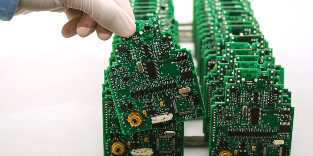
A Printed Circuit Board (PCB) utilizes copper conductors to establish electrical connections between various parts of an electronic assembly, while simultaneously providing mechanical support for electronic components to enable device integration into an enclosure. PCB design must incorporate a precise set of procedures compliant with manufacturing processes, integrated circuit packaging, and bare board structure.
Conductive elements on a PCB include copper traces, pads, and planes, among others. Conductor layers are laminated with insulating materials to form the mechanical structure. The entire assembly is typically coated with a non-conductive solder mask, and component identifiers are often screen-printed on its surface. Upon completion of manufacturing stages, the bare board proceeds to assembly, where components are soldered onto it, resulting in a PCBA ready for testing.
PCBs are critically important as they provide electrical connectivity between components, rigid support to secure components, and compact packaging suitable for integration into final products. PCB design has evolved into a specialized discipline within the electronics industry.
What is the Difference Between PWB and PCB?
Both PCB and PWB refer to circuit boards composed of one or more copper layers laminated onto a non-conductive plastic substrate, which connect and support components via conductive pathways. However, historical distinctions exist, as PWB denotes early printed circuit board types predating the development of more advanced PCB technologies.
During the nascent period of the electronics industry, circuit boards featured simple connections, making the designation “Printed Wiring Board” particularly appropriate. PWB forms the foundational basis for PCB, with the latter representing an upgraded terminology for circuit boards incorporating superior technology. The relationship between PWB and PCB parallels that between computer programs and software—capable of enhancement while maintaining effective backward compatibility. Their fundamental similarity stems from the fact that their differentiation primarily results from subsequent technological evolution.
In electronics technology’s early development phase, the term “Printed Wiring Board” was employed. Because board connections were merely point-to-point, using the PWB designation was considered appropriate during the industry’s initial phases.
A PWB represents a design substrate without installed components. Beyond etched drill holes, PWBs contain openings (e.g., pads) for soldering electronic components. The PWB transitions to a PCB only after undergoing a series of chemical and physical processes for component installation, because circuit functionality is significantly influenced by the printed circuit board’s design.
Subsequently, with advancements in circuit board technology, the compound term “Printed Circuit Board” was created. Initially, this term might have seen limited internal use; the word “circuit” proved more apt as printed circuit boards enabled more sophisticated functionalities. As technology progressed and PCB terminology gained widespread adoption, PWB usage in electronic pre-production gradually diminished.
Since printed circuit design substantially impacts functionality, the IPC Technical Activities Executive Committee mandated the exclusive use of the term PCB in all new documentation around 1999.
Regional variations also influence PWB and PCB usage. For instance, “Printed Circuit Board” sees more frequent use in the United States, whereas PWB is preferred in Japan. Japanese industry favors PWB over PCB to avoid confusion with the identical acronym for “Polychlorinated Biphenyls”—a specific toxic substance present in Japan.
Consequently, we can state that in most global regions, PWB constitutes an archaic term for PCB, while PCB serves as the universal terminology for bare circuit boards without mounted components.
PWB and PCB respectively denote Printed Wiring Board and Printed Circuit Board. Both terms refer to boards providing physical support and electrical connections for electronic components. Although commonly utilized in electrical and electronic devices, they exhibit distinct differences. Let us examine key aspects to deepen our understanding of their overlaps and distinctions.
Technical Differences Between PWB and PCB
A fundamental difference between PWB and PCB lies in the manufacturing technologies employed during assembly.
- PWB Technology: PWB refers to a substrate within electronic devices lacking complete circuit formation. It employs an epoxy-glass substrate without any pre-printed components. This older technology involves material etching during production to create connections, providing insulating surfaces between conductive traces. It encompasses manual drawing and etching of circuits onto the board, coupled with point-to-point component connection according to specific designs, ultimately forming electronic circuits for device creation.
- PCB Technology: PCB technology is more advanced, involving computer-aided design and circuit creation on boards. PCB manufacturing typically utilizes insulating boards with interconnected wiring. Components are printed onto dielectric substrates following predefined layouts that extend beyond simple point-to-point connections. Conductor dimensions and spacing profoundly influence circuit operation, far exceeding basic connectivity considerations.
What Materials Are Used in PWB and PCB Manufacturing?
Due to design similarities, PWB and PCB can employ comparable manufacturing materials. Depending on the circuit board’s application scenario, PWB and PCB might also utilize different materials. These boards comprise conductive and non-conductive layers. Non-conductive layers typically provide electrical isolation, while conductive layers facilitate signal transmission.
- Conductive Layer Materials: Conductive layers construct signal transmission paths on PWB and PCB. Commonly used conductive layer materials include copper, silver, and gold.
Despite gold’s superior conductivity and minimal resistance, its elevated cost restricts application. Copper serves as the preferred material for most PWB and PCB applications, offering advantageous cost-effectiveness and satisfactory conductivity. - Substrate Materials: Non-conductive layers consist of non-conductive materials. This layer typically incorporates ceramics, FR-4, composite epoxy resin materials, etc. These materials exhibit varying thermal conductivity and insulation properties. FR-4 sees extensive use in multiple configurations due to its versatile dielectric performance.
- Prepreg: Another material widely used in PWB and PCB is prepreg. It bonds layers together, particularly in board core sections. Comprising pre-resin-impregnated glass fiber, it becomes pliable under high temperatures, adhering to laminate surfaces before solidifying upon cooling to establish robust bonds.
- These boards additionally incorporate other materials like solder. Solder, typically used for component interconnection, primarily consists of lead and tin. Conductive pathways may receive surface coatings to prevent copper trace corrosion (e.g., from gold, nickel, silver, tin).
Other Terms Related to PWB and PCB
Beyond PCB and PWB, you might also encounter PCBA, CCA, PCA, and PWA. These terms also reference printed circuit boards.
PCBA abbreviates Printed Circuit Board Assembly. When a PCB undergoes assembly (component mounting), it becomes PCBA or PCB assembly. Following the 1999 terminology update, PCBA has become the universal term for all assembled circuit boards. From end-users to technical committees, PCBA remains the preferred terminology for assembled boards.
PWA stands for Printed Wiring Assembly. This constitutes an outdated term for PCB assembly or PCBA.
CCA represents Circuit Card Assembly. While technically identical to PCBA, CCA sees less frequent application.
PCA denotes Printed Circuit Assembly. PCA also equates to PCBA but now appears infrequently.
In summary, we conclude that PWB, PCB, and circuit cards are synonymous, referring to bare printed circuit boards; whereas PCA, CCA, PWA, and PCBA are equivalent, denoting assembled circuit boards.
Among these terms, PCB and PCBA enjoy the most widespread usage.
Application Scenarios and Their Impact on PWB vs PCB Selection
- PWB Applications: PWB functions as the foundation and framework for components interconnected manually or via cables. This may involve soldering, crimping, splicing, or alternative wiring methodologies. Its capacity for wire repositioning and rerouting over time facilitates design modifications without complete board replacement. Consequently, PWBs prove preferable in projects where flexibility represents a critical factor.
- PCB Applications: PCB architecture implements automated processes like etching and plating. Components mount directly onto boards rather than utilizing separate wiring, enabling higher component density within significantly reduced space compared to PWB capabilities. This enhances reliability by eliminating concerns regarding connection loosening through operational wear. However, PCB design modifications necessitate complete board replacement, since all components embed permanently. PCBs suit projects demanding high precision, repeatability, and minimal long-term maintenance.
Key Point: PCBs demonstrate considerably greater advancement and versatility than PWBs, owing to their capacity for supporting more complex circuits and broader component ranges.
Conclusion
Within the consumer electronics sector, PWB and PCB terminology sometimes appears interchangeably. Both Printed Wiring Boards (PWBs) and Printed Circuit Boards (PCBs) represent circuit types supporting and connecting electronic components. While constituting integral elements of all electronic devices, they serve distinct purposes regarding circuit implementation.
In conclusion, terminology application varies regionally, but the fundamental distinction resides in the circuitry itself. PCBs incorporate pre-etched circuits, enabling rapid, efficient mass production; conversely, PWBs lack this characteristic. Typically, the printed wiring board constitutes a fundamental PCB production step. The sophisticated circuit boards recognized today originated as PWBs; they have simply evolved to a stage necessitating PCB terminology. This breakthrough yielded numerous benefits for PCB manufacturing technology and research; however, it never effectively eliminated the PWB term, explaining both terms’ continued contemporary usage.


0 Comments