
Introduction
The proper operation of modern electronic systems relies fundamentally on power supply technology. As the cornerstone of all electronic designs, power supply circuits require precise understanding of their terminology as a prerequisite for developing functional projects.
Standard terms such as VCC, VEE, VDD, and VSS are ubiquitous in IC datasheets, design documentation, and schematics. Engineers must master these concepts thoroughly. These voltage naming conventions not only simplify circuit comprehension but are also crucial for interpreting the power supply and pin functions of integrated circuits, amplifiers, and other operational circuits.
This guide provides a comprehensive analysis of the technical meanings and roles of these terms in circuits. Mastering this knowledge will effectively enhance circuit performance optimization capabilities and ensure adherence to signal integrity design standards.
This article systematically explains the core differences between VCC, VEE, VDD, and VSS in electronic engineering by elaborating on their definition standards, key roles in circuit design, and practical application scenarios in integrated circuits, amplifiers, and microcontrollers, helping readers build a complete understanding of power supply labeling systems.
Fundamentals of Power Supply Voltage
All electronic circuits require stable power supply. Supply voltages serve both as energy sources for circuit operation and are closely related to the normal functioning of various components. Voltages in circuits are typically named and classified according to their function, source, or polarity.
For example, VCC represents the positive supply in Bipolar Junction Transistor (BJT) circuits, while VDD serves as the primary supply in MOSFET-based designs. VEE and VSS correspond to negative supply or ground references, with their specific meanings depending on whether the circuit employs BJT or MOSFET architectures.
During circuit design and debugging, correct voltage configuration not only ensures proper current transmission but also effectively protects sensitive components. In the PCB manufacturing stage, standardized voltage labeling and processing procedures directly determine the reliability and service life of circuit boards.
Detailed Explanation of the Four Voltage Designations
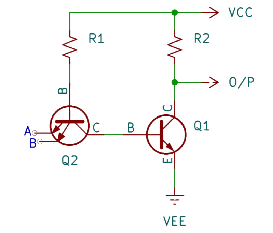
VCC – Originally stood for “Voltage at the Common Collector.” This term originates from bipolar transistor logic circuits, where the collector supply is typically connected to a positive voltage. Today, VCC generally refers to the positive supply voltage for any integrated circuit, particularly common in TTL (Transistor-Transistor Logic) based circuits.
VEE – Represents “Voltage at the Emitter,” corresponding to the negative supply connection in bipolar transistor systems, especially applied in ECL (Emitter-Coupled Logic) circuits. In other types of integrated circuits, this designation may refer to the most negative supply voltage in circuits utilizing both positive and negative power supplies.
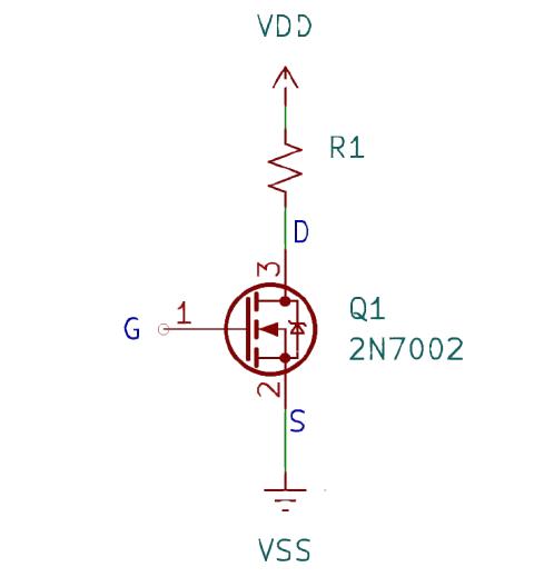
VDD – Traditionally meant “Voltage at the Drain.” This nomenclature derives from MOS transistor logic circuits, where the drain terminal is connected to the positive supply voltage. It has now become the standard designation for the positive supply pin in CMOS (Complementary Metal-Oxide-Semiconductor) integrated circuits.
VSS – Stands for “Voltage at the Source.” Similar to VDD, this term comes from MOS logic circuits, denoting the source terminal. VSS represents the ground pin (0V reference) in a circuit, serving as the most negative point in the power supply system and providing the return path for current to the power supply.
Core Differences Comparison
It is important to note that while both VCC and VDD denote positive supply voltages, VCC is predominantly used in TTL logic level contexts, whereas VDD is applied in CMOS logic level scenarios. Although VEE and VSS both serve as low-potential reference points, VEE typically appears as the negative voltage in dual-supply systems, while VSS is always associated with the system ground potential.
| Designation | Essential Meaning | Technical Context | Typical Application Areas |
|---|---|---|---|
| VCC | Common Collector Voltage | BJT Circuit Positive Supply | Analog Circuits/Microcontrollers/Signal Amplifiers |
| VDD | Drain Voltage | MOSFET Circuit Positive Supply | Digital Circuits/Microprocessors/Memory Chips |
| VEE | Emitter Voltage | BJT Circuit Negative Supply/Ground | Audio Amplification/Signal Processing Circuits |
| VSS | Source Voltage | MOSFET Circuit Ground Reference | Integrated Circuits/Digital System Grounding |
Terminology Value in Circuit Design
Importance of Standardized Labeling
Accurate labeling of voltage terms in datasheets, schematics, and other design documentation ensures:
- No risk of voltage parameter misinterpretation
- Precise pin assignment matching
- Enhanced system integration reliability
Technical risks that may arise from incorrect labeling
- Component damage: Misjudgment of voltage pins leading to overvoltage, damaging sensitive components such as transistors and amplifiers
- Stability degradation: Improper voltage distribution causing increased noise, resulting in circuit performance fluctuations
- Functional abnormalities: Incorrect voltage reference directly causing circuit failure or erratic behavior
Voltage Standards Across IC Families
- TTL Logic: Uses VCC as positive voltage, VEE as ground reference
- CMOS Technology: Uses VDD as positive voltage, VSS as ground reference
- Operational Amplifiers: Employs VCC and VEE combinations in dual-supply configurations
Cross-Domain Application Specifications
Microcontroller Systems
- Architecture differences: Labeled as VCC or VDD depending on internal BJT or MOSFET technology
- Stability requirements: Voltage fluctuations in real-time processing systems may cause system crashes
- Practical recommendation: Confirm supply specifications according to chip technical manuals
Audio Amplification Systems
- Technical key: VCC and VEE voltage accuracy determines transistor operating range
- Quality assurance: Precise voltage regulation eliminates distortion and noise interference
Mixed-Signal Circuits
- Interface design: Proper allocation of VDD and VEE maintains voltage level matching across circuit blocks
- Anti-interference strategy: Voltage domain isolation effectively reduces crosstalk between different PCB modules
Summary
Proficiency in the standardized application of VCC, VEE, VDD, and VSS represents a core competency for electronic design engineers. These terminology systems not only ensure accurate voltage configuration but also enable verification of BJT and FET operational status. Through deep understanding of these concepts, engineers can effectively avoid common design errors, enhance signal integrity, and construct highly reliable circuit systems.
Designers who accurately master these power supply terms will possess stronger circuit debugging and optimization capabilities, demonstrating outstanding problem-solving skills when dealing with complex circuits such as microcontrollers, embedded systems, and operational amplifiers.


0 Comments