
In the world of custom mechanical keyboards, we often talk about switches, keycaps, and case feel. However, hidden beneath all these components lies the true core that determines a keyboard’s functionality, reliability, and customizability: a green circuit board—the PCB. This article provides an in-depth yet accessible analysis of every aspect of the mechanical keyboard PCB.
What is a Mechanical Keyboard PCB?
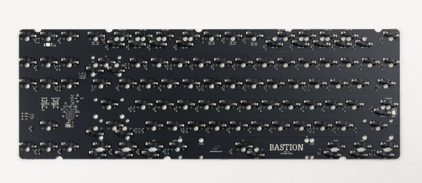
PCB stands for Printed Circuit Board. In a mechanical keyboard, the PCB is not just the substrate that carries all components; it is the “brain” and “central nervous system” of the entire keyboard.
Its core functions include:
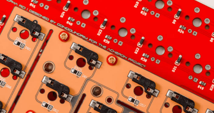
- Electrical Connection: Through intricate internal copper traces, it connects dozens or even hundreds of mechanical switches, LEDs, the main controller chip, USB port, and other electronic components into a complete circuit system.
- Signal Detection and Transmission: When you press a key, the two metal contacts of the switch connect two corresponding contact points on the PCB, forming a closed circuit. The main controller chip immediately detects this signal change, precisely identifies which key was actuated, encodes this information, and sends it to the computer via the USB cable.
- Support for Advanced Features:
- Hot-Swap: Utilizes special sockets pre-installed on the PCB, allowing for solder-free installation and removal of switches, greatly facilitating customization.
- RGB Backlighting: Provides independent circuits and control signals for each key’s LED, enabling dazzling lighting effects.
- Firmware Hosting: All the keyboard’s underlying logic (such as key mapping, macros, and lighting modes) is stored in the main controller chip on the PCB and can be updated by flashing new firmware.
Key Characteristics of a PCB:
- Layout: Determines the keyboard’s physical form factor (e.g., 60%, 75%, TKL) and whether it supports special key positions.
- Mounting Compatibility: Indicates whether it supports popular mounting styles like gasket mount, which can lead to a softer, more flexible typing feel.
- LED Orientation: Designed for north-facing or south-facing LEDs, which can affect the lighting performance of certain switches with light guides.
How is a Keyboard PCB Installed?
Different keyboards employ different mounting systems, but here is a brief overview of some common ones:
- Top Mount: The PCB is screwed into the top part of the keyboard case.
- Tray Mount: Similar, but the PCB is screwed into the bottom of the case. Tray-mounted keyboards can sometimes offer a less consistent typing feel because the screws may create uneven tension across the PCB.
- Gasket Mount: The keyboard uses foam or rubber gaskets (which may be attached to the PCB or the plate) placed between the case halves. This system typically provides a softer, more flexible, and bouncier typing sensation.
What Other Features Do Mechanical Keyboard PCBs Support?
- Stabilizer Support: Some PCBs allow for the addition of screw-in or snap-in stabilizers. These are generally superior to plate-mounted stabilizers and provide a better experience with larger keys like the Spacebar and Enter key.
- Hot-Swap Sockets: As mentioned, these sockets allow you to remove and replace switches without desoldering the entire board.
- RGB Lighting: You can either add RGB lighting to a PCB yourself or purchase one that already has this functionality built-in.
How is a Mechanical Keyboard PCB Manufactured?
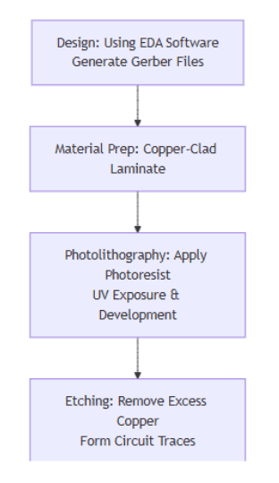
The manufacturing of a mechanical keyboard PCB is a complex process integrating precision machinery, chemistry, and electronic technology. The diagram below illustrates the core process flow:
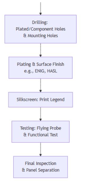
Detailed Explanation of Each Step:
- Design Output: Engineers use specialized software (EDA) to draw the circuit schematic and layout, generating standard Gerber and drill files, which serve as the “blueprint” for production.
- Material Preparation: The substrate is typically a Copper-Clad Laminate (CCL), which consists of an insulating fiberglass board laminated with a layer of copper foil.
- Photolithography: A light-sensitive photoresist is applied to the copper board. A film with the circuit pattern is placed over it, and the board is exposed to UV light. The exposed areas (in a positive process) undergo a chemical change and are subsequently dissolved in a developer, revealing the desired circuit pattern.
- Etching: The board is placed into an etching solution, which removes the exposed copper. The copper protected by the photoresist remains. The remaining photoresist is then stripped away, leaving only the designed copper traces.
- Drilling: High-precision CNC drilling machines create holes for switch pins, components, and standoffs based on the drill files.
- Plated Through-Hole (PTH) Process: The walls of the drilled holes are non-conductive. A thin layer of copper is chemically deposited onto the hole walls to electrically connect different layers, followed by electroplating to thicken the copper layer.
- Solder Mask Application: This is the familiar green (or other colors) layer. It is applied over the copper traces to provide insulation, prevent oxidation, and avoid short circuits. Using a process similar to photolithography, only the component solder pads are exposed.
- Silkscreen: White text and symbols are printed onto the board to identify component locations, orientations, etc.
- Surface Finish: The exposed solder pads undergo a protective treatment. Common methods include:
- ENIG (Electroless Nickel Immersion Gold): Excellent flatness, strong oxidation resistance. A common high-quality choice.
- HASL (Hot Air Solder Leveling): Low cost, good solderability, but less flat.
- Gold Plating: High cost but superior performance, excellent corrosion resistance and conductivity, often used for hot-swap sockets and high-end PCBs.
- Testing and Depaneling: Electrical tests are conducted to ensure no short or open circuits. Finally, individual PCBs are separated from the larger panel (via V-scoring or break-off tabs) and packaged for shipment.
A Case Study: How I Made a PCB Mechanical Keyboard
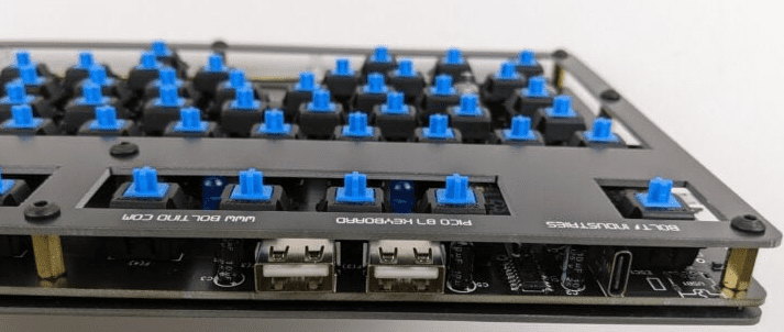
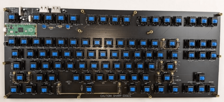
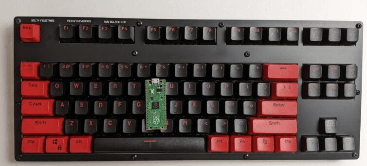
I created an 87-key mechanical keyboard with a traditional layout, constructed from three layers of FR-4 PCB material. While using PCB material for the entire case might seem unconventional, it is ideal—it’s sturdy, easy to customize, and very easy to clean. The keyboard’s unique aspect is its open-source firmware, written in the Arduino IDE, running on a Raspberry Pi Pico.
My Process Overview:
n short, I started by designing a layout, converted it into a schematic, and then placed the 87 keys in their correct positions on the PCB. After the layout was complete, I placed a diode near each switch. The circuit wasn’t complex, but the board was very large. I have open-sourced my schematics and layout so others can use or customize them without starting from scratch.
Designing the Layout:
- I recommend using keyboard-layout-editor.com to design your layout—a convenient tool for dragging, dropping, resizing keys, and customizing legends.
- Another useful tool is the Keyboard Firmware Builder (kbfirmware.com), which can generate a row-and-column matrix diagram from your layout data. However, I don’t recommend using its firmware generation feature as it’s outdated.
Schematic and PCB Layout in EDA Software:
- For EDA software, I recommend EasyEDA for beginners. It’s simple yet powerful.
- Find and use a CHERRY MX-style switch footprint—the gold standard for mechanical keyboard switches.
- Careful Labeling: Label each key meticulously in your schematic to avoid confusion (e.g., distinguishing “F1” the key from “F” the letter key).
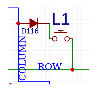
- The Keyboard Matrix: Since microcontrollers don’t have enough pins for every key, a matrix is used to scan rows and columns. Each switch requires a diode (1N4148 is the standard choice) to prevent “ghosting.” Diode orientation depends on the firmware.
- Key Spacing: The standard key spacing unit is 0.75 inches (750 mils). Set your grid accordingly. Larger keys (Spacebar, Shift, etc.) are multiples of this unit (e.g., 1.25u, 1.75u, 6.25u).
- Stabilizers: Add footprints for stabilizers (typically 6.25u for spacebar, 2u for Shift, Enter, etc.).
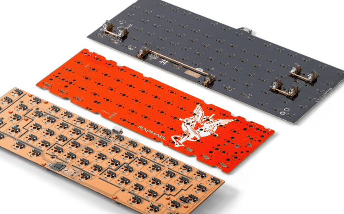
- Top and Bottom Plates: For a layered case, create FR-4 top and bottom plates. Copy the main PCB outline and keyhole pattern, then remove all non-mechanical elements. Use M3 screws, nuts, and standoffs to assemble the three layers.
Connecting to USB:
- While you can use the microcontroller’s USB port, I preferred adding a separate USB connector for better orientation.
- For a Raspberry Pi Pico, you can solder wires from a USB connector to the TP2 (D-) and TP3 (D+) test points on the bottom.
- Keep the D+ and D- traces parallel and of equal length.
- Recommended through-hole connectors for ease of soldering:
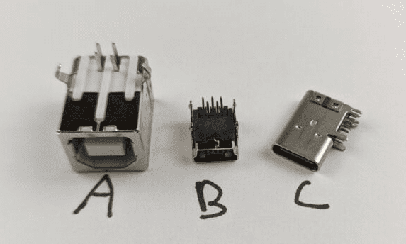
- USB-B (Valuepro USB-BF90): Large and easy to solder.
- USB-Mini B (Valuepro 920-462A2021D10102): Compact and manageable.
- USB-C (XKB U264-141N-4BAC10): Modern but challenging to solder. Requires 5.1kΩ pull-down resistors on each CC pin for proper operation with USB-C hosts.
Firmware:
- BMK (Bolt Mechanical Keyboard): A custom firmware that runs in the Arduino IDE, offering full customization and fun macro programming.
- KMK: A popular firmware that runs on CircuitPython, making it perfectly compatible with the Raspberry Pi Pico. Configuration is as simple as editing a text file on the Pico’s drive.
How are Mechanical Keyboard PCBs Tested?
Quality is the lifeline of PCBs, especially in the custom keyboard community. A qualified PCB must pass multiple rigorous inspection stages.
- In-Process Production Testing:
- Automated Optical Inspection (AOI): After etching and solder mask application, AOI equipment scans the PCB, comparing it to the design files to automatically detect micro-defects like breaks, shorts, gaps, or pinholes.
- Flying Probe / Bed of Nails Test:
- Flying Probe Test: Suitable for small batches. 2 to 8 high-speed probes move across the PCB surface, testing the conductivity and insulation of net points one by one.
- Bed of Nails Test: Suitable for mass production. A custom fixture with numerous spring-loaded pins makes contact with test points across the entire board simultaneously for rapid testing.
- Finished Product Functional Testing:
This is a mandatory step for keyboard manufacturers or kit vendors to ensure every shipped PCB functions correctly.- Short and Open Circuit Test: Using a multimeter’s continuity mode, spot-check or fully inspect for shorts between VCC and GND and verify connectivity between each switch pad and the corresponding microcontroller pin.
- Power-On Test:
- Basic Power: Connect to a computer to check if it is recognized by the OS and if the USB connection is stable.
- Key Actuation Test: Using tweezers or a test switch, short-circuit the two solder pads for each key position and observe if the correct key input is registered on the computer. This is crucial for verifying every key circuit.
- LED Backlight Test: If the PCB supports backlighting, test every LED position for functionality, correct color, and proper effect switching.
- Other Functionality Tests: Test onboard EEPROM (for saving settings), reset buttons, jumpers, etc.
- Visual and Physical Inspection:
- Check for burrs or delamination on the PCB edges.
- Inspect the solder mask for uniformity, scratches, or bubbling.
- Check solder pads for oxidation or obvious damage.
- Verify that hot-swap sockets are installed flush and securely.
Conclusion
For a mechanical keyboard, the PCB is the bridge connecting physical input to the digital world. Its quality directly determines the keyboard’s stability, functionality, and lifespan. From design and manufacturing to final inspection, every step involves precise engineering. Whether for keyboard manufacturers or perfection-seeking enthusiasts, a deep understanding of the PCB is an essential step on the path to building the perfect keyboard.


0 Comments