
Introduction
In today’s landscape where electronic devices relentlessly pursue thinner profiles, higher integration, and greater reliability, traditional rigid printed circuit boards (PCBs) can no longer meet the demands of all applications. It is precisely this trend that has given rise to Flexible Printed Circuit Boards (Flex PCBs). With their unique ability to bend and fold, flex PCB technology breaks through the physical limitations of traditional electronic interconnects, opening up new dimensions for product design. From satellites soaring in space to the smartphones in our pockets, flex PCBs are quietly reshaping the form and future of electronics with their irreplaceable advantages. This article will provide an in-depth look at the definition, principles, types, and structure of flex PCBs, unveiling the core secrets of this key technology.
What is a Flex PCB?
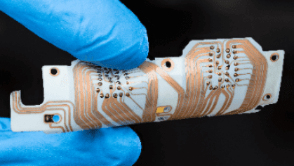
A Flexible Printed Circuit Board (Flex PCB), often referred to as a flex circuit, flex board, or FPC, is an electronic interconnect fabricated using a flexible insulating substrate, such as polyimide (PI) or polyester. Its conductive pathways are formed from copper foil etched onto this flexible base, and electronic components are soldered onto exposed copper pads.
The core advantage of a flex PCB over its rigid counterpart lies in its physical properties: it can bend, twist, and flex. This not only grants greater design freedom but also significantly enhances the reliability and robustness of the overall electronic system by reducing the need for connectors and discrete wiring. Depending on the number of conductive layers, flex PCBs can be categorized into single-sided, double-sided, or multilayer structures to meet varying circuit complexity requirements.
Applications and Advantages of Flex PCBs
The applications of flex PCBs fall into two main categories: firstly, serving as fully functional circuit boards for mounting various electronic components; and secondly, acting as flexible connecting cables enabling three-dimensional electrical interconnections within a device.
Their primary application advantages include:
- Dynamic Flexibility: Capable of withstanding hundreds of thousands of repeated bending cycles, making them ideal for continuously moving parts like hard disk drive heads, folding phone hinges, and robotic joints.
- Space Savings: Their thin, lightweight nature allows for routing in tight or irregularly shaped spaces, optimizing internal device layout.
- Lightweight Design: A single flex circuit can effectively reduce overall weight compared to solutions using multiple rigid boards and wire harnesses.
- High Reliability: The reduction of mechanical connection points, such as board-to-board connectors, lowers the risk of connection failure and improves system stability.
Consequently, flex PCBs have expanded from their initial use in high-end sectors like aerospace and defense to widespread adoption in consumer products such as smartphones, wearables, automotive electronics, and medical devices.
How Flex PCBs Work and Their Structure
Electrically, the operating principle of a flex PCB is fundamentally the same as that of a rigid PCB, with the core function being signal transmission via copper traces. The fundamental difference lies in their physical structure.
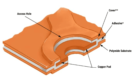
- Substrate: Flex PCBs use bendable films like polyimide as the base material, whereas rigid PCBs typically use non-flexible FR-4 (glass fiber epoxy).
- Coverlay: Flex PCBs commonly use a coverlay—a flexible polyimide layer laminated with adhesive—to protect the circuits. Rigid PCBs use a solder mask.
- Stiffeners: To provide localized support in specific areas (e.g., where connectors are mounted), flex PCBs often have FR-4 or stainless steel stiffeners adhesively bonded to them.
Main Types of Flex PCBs
Single-Sided Flex PCB
This is the simplest and most cost-effective flex PCB structure. It features a single conductive copper layer, with components concentrated on the opposite side. Its simple structure and economy make it widely used in cost-sensitive electronics with less complex circuits.
Double-Sided Flex PCB
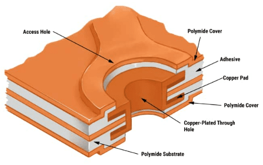
This type features copper foil on both sides of the base substrate, with electrical connections between the two layers achieved through plated through-holes (PTHs). This structure suits more complex circuit designs and is common in automotive dashboards, industrial controls, and high-end consumer electronics.
Multilayer Flex PCB
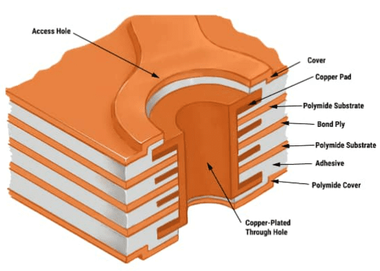
Consisting of three or more conductive layers laminated together, these layers are isolated by dielectric layers and interconnected using vias. Multilayer flex PCBs offer extremely high design freedom and integration density. They are primarily used in space-constrained, highly integrated devices like smartphone mainboards, camera modules, and military communication equipment.
Detailed Structural Analysis of a Flex PCB
Using the most basic single-layer flex PCB as an example, its structure is primarily composed of the following layers, from top to bottom:
- Silkscreen: The legend printed on the coverlay, used for marking component designators, version information, etc.
- Coverlay: Equivalent to the solder mask on a rigid board, it protects the copper traces from oxidation, damage, and short circuits. It is typically made of a polyimide film and adhesive.
- Conductive Copper Foil: The core conductive layer etched to form the circuit traces.
- Substrate: The carrier for the circuit, providing insulation and mechanical support. The most common material is heat-resistant polyimide (PI).
- Adhesive: Used to firmly bond the copper foil to the substrate and to achieve lamination in multilayer boards. The thickness and type of adhesive can affect the circuit’s flexibility and thermal performance.
Summary
With their unique bendability and exceptional spatial adaptability, Flex PCBs have become an indispensable element in the innovative design of modern electronics. Through precise materials science and manufacturing processes, complex circuit networks are constructed on flexible films, successfully achieving a perfect balance between reliability, lightweight design, and freedom in three-dimensional routing. From simple single-layer interconnects to highly integrated multilayer circuits, the technological spectrum of flex PCBs continues to expand, consistently driving electronic devices toward a future that is thinner, more durable, and more diverse in form factor. Understanding and mastering flex PCB technology is crucial for any engineer or decision-maker committed to cutting-edge electronic product development.


0 Comments