
Introduction
Success in PCB board prototyping requires a meticulous approach to the entire product development cycle. This encompasses everything from initial schematic capture and component placement to advanced considerations of signal integrity (SI) and power distribution network (PDN) design during the PCB board prototyping phase, ultimately determining the prototype’s success.
Phase 1: Pre-Design – Systems Engineering & Requirements Definition
Before launching any EDA tool, thorough system planning is the cornerstone of project success.
- System Requirements & Functional Spec Definition
- Define Electrical Parameters: Clarify the board’s input/output voltages, current capacity, power budget, signal types (analog, digital, high-speed, differential), and key performance metrics (e.g., SNR, bandwidth, drive capability).
- Standardize Interface Protocols: Identify all external interfaces (e.g., USB 2.0/3.0, HDMI, Ethernet, UART, I²C, SPI) and ensure their electrical characteristics comply with relevant protocol standards.
- Core Component Selection & Pre-validation
- Key IC Selection: When choosing microcontrollers, processors, or FPGAs, consider not only processing power but also the soldering feasibility of their recommended PCB package. BGA packages offer superior performance but are difficult to inspect; QFP/TSSOP packages are more suitable for prototyping and debugging.
- Component Availability & Lifecycle: Check the supplier’s PCN to confirm selected components are in active production, avoiding soon-to-be-obsolete parts.
- Create an Accurate Component Library: Strongly recommend creating or verifying schematic symbols and PCB footprints based on official datasheets. Incorrect footprint pad sizes or spacing is the primary technical risk causing complete prototype batch failure.
- Mechanical Structure & Thermal Design Planning
- Form Factor & Mounting Holes: Use professional MCAD software for collaborative design, or at minimum, provide a precise DXF outline file to the PCB layout engineer.
- Thermal Management Strategy: Identify high-power dissipation devices (e.g., LDOs, PAs, motor drivers). Plan thermal paths early, considering the need for thermal vias, thermal pads, or external heatsinks.
Phase 2: Engineering Design Flow – Precise Translation from Logical to Physical Implementation
This phase is the technical core, determining the circuit’s final performance and reliability.
- Schematic Capture: Building the Logical Foundation
- Modular & Hierarchical Design: Organize the circuit into clear functional blocks (e.g., Power Management, MCU Minimum System, Sensor Interface, Comm Module), enhancing readability and maintainability.
- Circuit Simulation & Verification: Perform SPICE simulation on critical analog circuits (e.g., op-amp filters, power supply feedback loops) or high-speed digital circuits to predict performance and identify issues early.
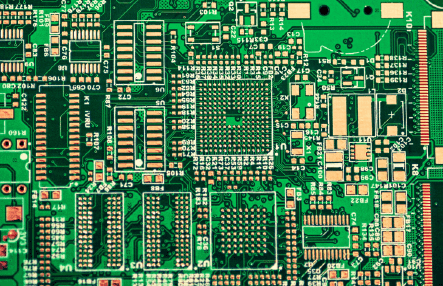
- PCB Layout: The Physical Realization of Electrical Performance
- Layout Priority Strategy:
- Primary: Place connectors, switches, and other fixed-location mechanical components.
- Secondary: Place core ICs and their associated decoupling capacitors, crystal oscillators, and other critical passive components.
- Follow Signal Flow: Component placement should generally follow the “input → processing → output” signal path, avoiding unnecessary crossings and reflow paths.
- Power Distribution Network Design:
- Use power planes or wide traces to provide low-impedance power paths for digital ICs.
- Place decoupling/bypass capacitors (typically a 100nF & 10uF combination) as close as possible to the IC’s power pins, with the shortest possible return path (to ground) to effectively suppress high-frequency noise.
- Layout Priority Strategy:
- PCB Routing: The Key to Signal Quality
- Routing Rule Definition:
- Trace Width Calculation: Based on current-carrying capacity (per IPC-2152 standard) and allowable temperature rise, use an online PCB trace width calculator to determine widths for power and ground traces. Example: 1A current typically requires 20-40mil (0.5-1.0mm) width for 1oz copper.
- Impedance Control: For high-speed signals (e.g., USB differential pairs, LVDS), controlled impedance routing is mandatory. Calculate and specify trace widths based on stack-up to match target impedance (e.g., 90Ω diff, 50Ω single-ended).
- Grounding System Design:
- For digital circuits, a solid ground plane is optimal, providing minimal return inductance and excellent noise immunity.
- For mixed-signal circuits, employ a partitioned but non-split strategy, isolating sensitive analog and noisy digital areas in layout, but connecting the ground plane at a single point to prevent ground loops.
- Design Rule Check & Manufacturing Validation:
- Before releasing manufacturing files, run a strict DRC based on the PCB fabricator’s process capabilities (min trace width/spacing, min drill size, copper-to-edge clearance).
- Perform a final visual check of the generated Gerbers using a viewer tool to ensure no layer misregistration, missing, or erroneous data.
- Routing Rule Definition:
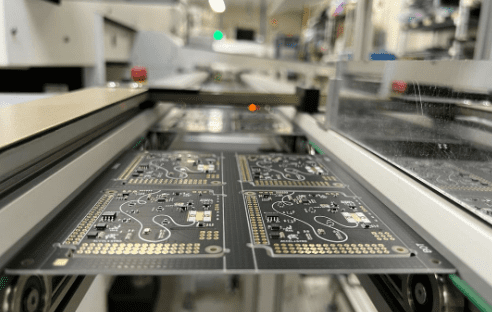
Phase 3: Fabrication & Procurement – Translating Design into Physical Reality
- Generating the Manufacturing File Package
- Gerber Files (RS-274X format): Includes all signal layers, power/ground planes, solder mask, silkscreen, and solder paste layers.
- NC Drill Files: Provides coordinates and sizes for all through-holes and vias.
- IPC Netlist File: Used by the manufacturer for Flying Probe Test to verify connectivity against the design.
- Assembly Drawing & Bill of Materials: Provides guidance for subsequent PCBA.
- Choosing a Prototype Service & Process Parameters
- Laminate Selection: Use standard FR-4 for general prototypes; consider high-frequency laminates for RF applications.
- Surface Finish Selection:
- HASL (Lead-Free): Low cost, good solderability, but poorer surface planarity.
- ENIG: Flat surface, suitable for BGAs and fine-pitch components, excellent oxidation resistance, higher cost.
- Immersion Tin/Silver: Alternatives to ENIG, offering good solderability and planarity.
- Solder Mask & Silkscreen: Choose high-contrast colors for better visibility during soldering and debugging.
Phase 4: Assembly & Test Validation – Achieving Functionality & Reliability
- Component Soldering
- Manual Soldering: Suitable for through-hole components and large-pitch SMDs. ESD protection is critical.
- Solder Stencil & Reflow Soldering: The standard process for SMT assembly. Use a laser-cut stencil to apply solder paste precisely, then solder using a reflow oven following an exact temperature profile to ensure reliable solder joints.
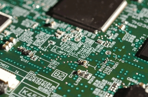
- Pre-Power-On Inspection & Testing
- Visual & Optical Inspection: Check for bridges, cold joints, misalignment, reversed polarity, etc.
- Short-Circuit Test: Using a DMM, measure resistance between all power nets and ground nets before applying power to ensure no low-resistance shorts.
- Insulation Resistance Test: For high-voltage sections, use a megohmmeter to verify dielectric strength.
- Systematic Power-On & Debugging
- Safe Power-On: Use a programmable DC power supply. Set the voltage slightly below the nominal value and enable current limiting (e.g., 50mA). Ramp up voltage slowly while monitoring current draw.
- Power Sequencing & Ripple Measurement: Use an oscilloscope to verify correct power-up sequencing and measure noise and ripple on power rails (typically <50mVpp).
- Module-by-Module Debugging:
- Verify accuracy of all power supply voltages.
- Test clock circuits (e.g., crystals) for correct oscillation frequency and amplitude.
- Program a simple test firmware to verify MCU operation.
- Test each peripheral functional module sequentially (sensor read, communication interfaces, etc.).
Professional Pitfall Avoidance & Design Wisdom
- Pitfall 1: Ignoring Datasheet Layout Guidelines. Application notes and recommended layouts from IC manufacturers are validated golden rules and must be strictly followed, especially for switch-mode power supplies, RF, and analog front-ends.
- Pitfall 2: Poor Power Supply Decoupling. The value, quantity, and placement of decoupling capacitors directly impact system stability. Each power pin should have a dedicated, closely placed decoupling capacitor.
- Pro Tip 1: Implement “Design for Test”. Include test points for measuring critical signals and power nets during layout. For complex systems, consider incorporating debug interfaces like JTAG/SWD.
- Pro Tip 2: Embrace Iteration, Include Redundancy. A perfect first-time prototype is rare. Include alternative component footprints for critical circuits (e.g., feedback resistors, filter caps) to provide debugging flexibility. Order 3-5 bare boards initially to accommodate potential assembly failures or design revisions.
Summary
Success in PCB board prototyping requires a meticulous approach to the entire product development cycle. This encompasses everything from initial schematic capture and component placement to advanced considerations of signal integrity (SI) and power distribution network (PDN) design during the PCB board prototyping phase, ultimately determining the prototype’s success.


0 Comments