
Introduction
In the realm of printed circuit board (PCB) design and manufacturing, the transition from digital layout to physical board hinges on a critical element: the PCB Gerber file. This comprehensive guide delves into the intricacies of the Gerber format – the industry-standard data format that bridges the gap between design intent and manufacturing execution.
When preparing your PCB design for production, the fundamental question arises: how does CAD layout data transform into precise manufacturing instructions? The answer lies in generating output files in the appropriate format. While contemporary design environments offer multiple output options including ODB++ and IPC-2581, the PCB Gerber file remains the ubiquitous choice for the majority of fabrication projects.
This guide explores what constitutes a PCB Gerber file, examining its technical composition, layer structure, and the vital manufacturing data it conveys. We will analyze Gerber data through both textual and graphical representations, demonstrating how manufacturers leverage this information throughout the PCB fabrication process. Understanding the PCB Gerber file format is essential for any designer seeking to ensure manufacturing accuracy, avoid costly errors, and streamline the transition from design to production.
Gerber Files: The First Step in the PCB Fabrication Process
When designing a printed circuit board in a CAD system, you see all the different materials and elements on the board represented by lines and shapes of various styles. Somehow, these graphical images need to be reformatted into data that a PCB fabrication company can use to create the bare circuit board. This front-end task in the PCB fabrication process is accomplished using Gerber files.
So, What is a Gerber File?
A Gerber file stores all the shape and positional data for each element in the printed circuit board layout. Typically, each layer from the PCB layout data will be placed in its own Gerber file. The concept is that separate layers can be used to prepare the stencils for each step in the fabrication and assembly process. In some cases, such as creating a drill drawing or a Gerber fabrication drawing, multiple layers can be combined into a single file by mirroring mechanical layers into the Gerber output.
Regarding the data stored in a Gerber file, it is human-readable, though not necessarily human-interpretable. Gerber file data is stored in an ASCII text file and includes the following four elements:
- Configuration Parameters
- Aperture Definitions
- XY Coordinate locations for draw and flash commands
- Draw and Flash command codes
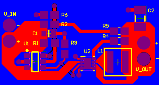
If you take all layers together and stack them in a composite view using a Gerber viewer application, you will get something similar to the simple example shown below.
In this view, we can clearly see that the Gerber viewer’s role is to recreate the PCB layout view, much as you would see it in your ECAD software. This is the view manufacturers use for a preliminary inspection of the board before providing a quotation. More specialized CAM software dedicated to Gerber files can be used to perform various DFM checks primarily involving clearances; these will then report any required updates back to you before PCB fabrication proceeds.
A Detailed Look at Gerber PCB Layers
In the following subsections, we will examine these Gerber file layers in detail:
- Top Silkscreen
- Top Solder Mask
- Top Copper
- Bottom Copper
- Bottom Solder Mask
- Bottom Silkscreen
- Outline / Mechanical
- Drill
- Internal Copper
Top Silkscreen (GTO)
- Purpose: The Top Silkscreen Gerber file contains the data to be printed, typically as white or black text on the board, such as part designators, component outlines, logos, polarity indicators, etc.
- Note: This layer is optional. It is perfectly acceptable to have a PCB without silkscreen if you so desire.
Top Solder Mask (GTS)
- Purpose: Contains the data for the protective solder mask layer that protects the copper. This is typically a green film but can be available in various colors.
- Note: The solder mask is negative, meaning the filled areas correspond to openings where solder mask will not be applied. These filled areas in the Gerber solder mask will leave the copper exposed in the final product. This exposed copper is used for component connection and test access points.
Top Copper Layer (GTL)
- Purpose: Contains data for all areas that require copper, including traces, pads, copper pours, vias, plated through-holes, etc.
- Note: All filled areas correspond to plated copper regions.
Bottom Copper Layer (GBL)
- Purpose: Same as Top Copper, but mirrored horizontally about the Y-axis.
- Note: All filled areas correspond to plated copper regions.
Bottom Solder Mask (GBS)
- Purpose: Same as Top Solder Mask, but mirrored horizontally about the Y-axis.
- Note: The solder mask is negative, meaning the filled areas correspond to openings where solder mask will not be applied. These filled areas in the Gerber solder mask will leave the copper exposed in the final product. This exposed copper is used for component connection and test access points.
Bottom Silkscreen (GBO)
- Purpose: Same as Top Silkscreen, but mirrored horizontally about the Y-axis.
- Note: This layer is optional. Many single-sided PCBs have no silkscreen on the bottom side.
Outline (GKO) and Mechanical Layers (GML)
- Purpose: Contains the board outline, any cutouts, V-scores, panel outlines, labels, etc. Without this layer, the manufacturer does not know how to cut the individual PCBs from the larger panels typically used in fabrication.
- Note: Mechanical elements should be contained within a single outline layer to prevent any features from being missed, unless it makes the outline unclear.
Drill Layer (DRL)
- Purpose: Contains all drill hole locations along with hole and via sizes. Drill files have many file extensions, including .txt or .drl. This layer file must not be confused with a drill drawing or drill map file. Technically, it is not a Gerber file.
- Note: Some EDA software may export separate files for plated and non-plated holes (vias). This is largely insignificant, as whether a hole is plated depends on the copper layers.
Internal Copper Layers (GT#)
- Purpose: Multi-layer boards may contain additional copper layers for signals or planes (ground or power) between the top and bottom copper layers.
- Note: Internal plane layers may be in negative format, meaning filled areas represent the absence of copper.
Gerber Filenames
| File Name | Type | Remarks/Description |
|---|---|---|
| Gerber_BoardOutline.GKO | Outline file | The PCB board factory cuts the board shape according to this file. The slots and solid-filled non-copper-plated through holes drawn by Jialichuang EDA are reflected in the border file after Gerber is generated. |
| Gerber_TopLayer.GTL | PCB Top Layer | Top Copper Foil Layer |
| Gerber_BottomLayer.GBL | PCB bottom layer | Bottom copper foil layer |
| Gerber_InnerLayer1.G1 | Inner copper foil layer, signal layer type. | |
| Gerber_InnerLayer2.GP2 | Inner copper foil layer, inner electrical layer type | |
| Gerber_TopSilkLayer.GTO | Top silkscreen layer | |
| Gerber_BottomSilkLayer.GBO* | Bottom silkscreen layer | |
| Gerber_TopSolderMaskLayer.GTS | Top Solder Mask Layer | It can also be called the window opening layer. By default, the board is covered with oil, and the elements drawn on this layer correspond to the area of the top layer, which is not covered with oil |
| Gerber_BottomSolderMaskLayer.GBS | Bottom Solder Mask | It can also be called the window layer. The board is covered with oil by default, and the elements drawn on this layer correspond to the area of the bottom layer without oil |
| Drill_PTH_Through.DRL | metallization drilling layer | This file shows the drill hole position that needs metallization on the inner wall, such as multi-layer pads, vias |
| Drill_PTH_Through_Via.DRL | via metallization drilling layer | This file shows the drill hole position that needs metallization on the inner wall, this file for JLCPCB use |
| Drill_NPTH_Through.DRL | Non-metallized drilling layer | This file shows the drill hole position that does not need metallization on the inner wall, such as through holes |
| Gerber_TopPasteMaskLayer.GTP | Top layer flux layer | For stencil opening |
| Gerber_BottomPasteMaskLayer.GBP | Bottom layer of soldering flux | For stencil opening |
| Gerber_TopAssemblyLayer.GTA | Top Assembly Layer | Only for reading, does not affect PCB manufacturing. Former name: ReadOnly.TopAssembly |
| Gerber_BottomAssemblyLayer.GBA | Bottom assembly layer | Only for reading, does not affect PCB manufacturing. Former name: ReadOnly.BottomAssembly |
| Gerber_MechanicalLayer.GME | Mechanical Layer | Only for reading, does not affect PCB manufacturing by default. Former name: ReadOnly.Mechanical. The information recorded in the mechanical layer in the PCB design is only for information recording. For example: process parameters, V-cut path, etc. |
| Gerber_DocumentLayer.GDL | Document Layer | Used to record PCB remarks, not involved in manufacturing |
Gerber File Formats
Over time, the Gerber file format has evolved in terms of data structure, but they all achieve the ultimate goal of replicating the board and creating stencils for fabrication. There are three basic Gerber file formats:
- RS-274-D
- RS-274-X
- Gerber X2 Format
- Gerber X3 Format
The original Gerber files were known as the RS-274-D format. These early files consisted only of XY coordinate locations along with draw and flash commands. As PCB designers, we had to manually assign aperture codes during the Gerber file creation process. Later, all aperture data, along with configuration parameters, would be extracted into a separate file. Careful effort was required to assign the correct codes to create accurate Gerber files for PCB fabrication.
If you are generating Gerber files for PCB fabrication from a CAD system today, you are likely using the RS-274-X format. This version consolidates all four elements of Gerber data (configuration parameters, apertures, XY coordinates, draw and flash commands) into a single file. The layer function is defined by the file extension. You will also note that your CAD system most likely assigns aperture positions automatically, eliminating the potential for human input error.
In recent years, newer versions of the Gerber format have become available, incorporating additional data. Gerber X2 files include information such as the layer function of the file, object attributes like pad types, locations for impedance-controlled traces, and more. Regarding layer function, this information is written inside the file itself, rather than relying on a specific file extension to denote the layer type. The goal is to enhance the Gerber format to make it more database-like, similar to ODB++, while retaining the traditional capability to drive photoplotters and LDI systems.
What Does Understanding This Mean for Designers?
Most PCB design packages can export Gerber files, even if they lack a built-in Gerber plot viewer or Gerber comparison functionality. As a PCB designer, your job is to ensure you understand the basic Gerber file extensions, what data is contained in the different Gerber files, and to briefly review them before sending the Gerbers for fabrication. Some manufacturers may still require separate aperture lists or other data files, and you need to know their purpose and how to create them. A quick review of your Gerber plot files before sending them for manufacturing can help you catch any errors that could delay fabrication or cause the finished boards to fail entirely.
Summary
This guide on PCB Gerber files is far more than a technical note; it profoundly illuminates the critical bridge connecting virtual design and physical reality. Serving as the “ultimate blueprint” for PCB design and the “universal language” of the manufacturing process, Gerber files precisely encode the designer’s digital vision—every trace, every pad, every layer of material—into machine-executable instructions. Understanding their layered structure, data composition, and format evolution is a core competency that every PCB designer must possess. This is not only a technical prerequisite for ensuring the lossless transfer of design intent and avoiding costly manufacturing errors but also a crucial step in the transition from a circuit designer to an engineering product creator with a comprehensive process perspective. It reminds us that exceptional products are born not only from innovative design but also rely on a profound insight and precise control over the path to realization.


0 Comments