
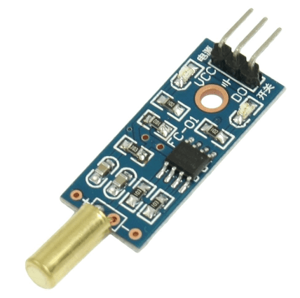
What is a PCB Sensor?
A PCB sensor is a critical component in electronic devices, enabling them to perceive, measure, and respond to changes in their environment, such as detecting temperature, pressure, motion, and humidity. These sensors are directly integrated onto the Printed Circuit Board (PCB), resulting in compact, efficient, and reliable devices.
Key Components of a PCB Sensor Board
- Sensing Element
This is the core of the sensor system, which directly detects physical parameters such as temperature, pressure, gas concentration, or touch. - Signal Conditioning Circuit
The output from the direct sensing element is often weak and noisy. Signal conditioning shapes the signal before it is digitized. - ADC (Analog-to-Digital Converter)
Since most processors only handle digital information, analog sensor signals require conversion. This is accomplished by an Analog-to-Digital Converter (ADC), which transforms continuous analog voltages into discrete digital values. - Interface with Microcontroller or Processor
A Microcontroller (MCU) or processor decodes and interprets the digitized signals. - Power Supply and Regulation
Most sensors and integrated circuits require stable voltage levels. A noise-free and stable power supply is crucial, especially for analog sensors.
Types of PCB Sensors
PCB sensors come in various types, each designed to measure specific physical quantities. Some of the most common types include:
Temperature Sensors
PCB temperature sensors are used to measure the temperature of a specific object or environment. They can be based on various sensing elements, such as thermistors, Resistance Temperature Detectors (RTDs), or thermocouples.
| Sensor Type | Working Principle | Temperature Range | Accuracy |
|---|---|---|---|
| Thermistor | Resistance change with temperature | -90°C to 130°C | ±0.1°C to ±1.5°C |
| RTD | Resistance change with temperature | -200°C to 850°C | ±0.1°C to ±1°C |
| Thermocouple | Voltage generated by temperature difference | -270°C to 1,260°C | ±0.5°C to ±2°C |
Pressure Sensors
PCB pressure sensors are used to measure the pressure of gases or liquids. They can be based on various sensing elements, such as piezoresistive strain gauges, capacitive sensors, or piezoelectric sensors.
| Sensor Type | Working Principle | Pressure Range | Accuracy |
|---|---|---|---|
| Piezoresistive | Change in resistance upon applied pressure | 0 to 100,000 psi | ±0.1% to ±0.5% |
| Capacitive | Change in capacitance with applied pressure | 0 to 10,000 psi | ±0.1% to ±0.5% |
| Piezoelectric | Voltage generated by applied pressure | 0 to 100,000 psi | ±0.5% to ±2% |
Humidity Sensors
PCB humidity sensors are used to measure the water vapor content in the air. They can be based on capacitive or resistive sensing elements.
| Sensor Type | Working Principle | Humidity Range | Accuracy |
|---|---|---|---|
| Capacitive | Change in capacitance with humidity | 0% to 100% RH | ±2% to ±5% RH |
| Resistive | Change in resistance with humidity | 0% to 100% RH | ±2% to ±5% RH |
Light Sensors
PCB light sensors are used to measure light intensity in a specific environment. They can be based on photodiodes, phototransistors, or photoresistors.
| Sensor Type | Working Principle | Spectral Range | Response Time |
|---|---|---|---|
| Photodiode | Current generated by incident light | 190 to 1,100 nm | 1 ns to 100 ns |
| Phototransistor | Amplification of incident light current | 400 to 1,100 nm | 1 μs to 100 μs |
| Photoresistor | Resistance change caused by incident light | 400 to 1,000 nm | 1 ms to 100 ms |
Applications of Sensor PCBs
| Field | Primary Applications | Sensor Examples |
|---|---|---|
| IoT Nodes | Environmental Monitoring, Smart Home Systems | Temperature/Humidity, Light, Air Quality, Motion, Door/Window, Leak Detection |
| Industrial Automation | Process Control, Machine Health Monitoring | Pressure, Flow, Level, Vibration, Temperature, Proximity, Encoders |
| Consumer Electronics | Smartphones, Wearables | Accelerometer, Gyroscope, Ambient Light, Proximity, Heart Rate, SpO₂, Motion |
| Automotive Electronics | Engine Control, Safety Systems, ADAS | Pressure, Temperature, O₂, TPMS, Airbag Accelerometer, Radar, Camera, Ultrasonic |
| Medical Devices | Vital Signs Monitoring, Diagnostic Equipment | ECG Electrodes, SpO₂ Probes, Temperature, Biosensors |
| Environmental & Agri-Tech | Climate/Soil Monitoring, Precision Agriculture | Soil Moisture, pH, Light Intensity, Weather Station Sensors |
Why Choose PCB Sensors?
- Unparalleled Precision and Reliability: In critical sectors like aerospace and defense, where measurement accuracy is paramount to success and safety, PCB sensors are trusted by top-tier clients worldwide for their near-absolute reliability.
- Excellent High-Frequency Response Characteristics: Piezoelectric technology is inherently suited for measuring rapidly changing dynamic signals, making PCB sensors exceptional at capturing transient events such as impact and explosion.
- Rugged Durability: Designed to withstand harsh industrial environments, including high temperatures, high humidity, and strong electromagnetic interference.
- Plug-and-Play Convenience: Thanks to ICP® technology, users avoid the need for complex external charge amplifiers, significantly reducing system integration difficulty and cost.
- Powerful Technical Support and Global Service Network: PCB provides in-depth technical consultation and calibration services, ensuring users consistently obtain accurate data.
How to Build a PCB Sensor Module: A Step-by-Step Guide
Step 1: Define Requirements
The first step in designing a PCB sensor module is to clarify the functional and environmental requirements. This determines the physical parameters to be measured (e.g., temperature, pressure, or motion), calibration range, required accuracy, resolution, response time, and any environmental conditions such as temperature range, humidity, or electromagnetic compatibility. Mechanical constraints, including board size, shape, and mounting location/method, must also be considered at this stage.
Step 2: Select the Correct Sensor Type
Therefore, selecting the appropriate sensor requires consideration of the chosen parameter combination and its intended application. Performance characteristics such as sensitivity, linearity, and power consumption must meet the specific application’s requirements. Furthermore, the interface (analog or digital), size, and availability and compatibility with other circuits must also be considered.
Step 3: Schematic Design
Next, the sensor is added to the schematic circuit within the chosen EDA tool (e.g., Altium Designer, KiCad, or Autodesk Eagle). Proper integration defines the electrical connections, utilizes suitable signal conditioning components (amplifiers, filters, ADC), and even implements voltage protection where appropriate.
Step 4: PCB Layout
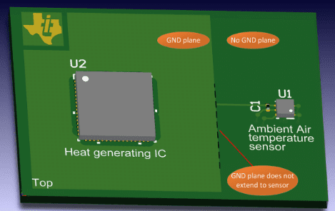
To minimize noise and crosstalk, ground planes, shielding, and careful trace routing are essential. Short, straight traces are advisable for analog sensors. Differential signal routing can be employed if needed. For high-precision designs, thermal management via via stitching and EMI protection must be considered.
Step 5: Simulation and Prototyping
Circuit simulation involves analyzing signal behavior stability and responsiveness under nominal operating conditions. Signal integrity, thermal performance, and power distribution must be simulated. Subsequently, a physical prototype is developed and built for validation under real environmental conditions. This step allows for testing under practical conditions to verify performance, stress tolerance, and mechanical fit.
Step 6: Testing and Calibration
Once the sensor is assembled, it must be tested. Testing includes load measurement, response time, resolution, linearity, and accuracy across the entire load range. From a robustness perspective, environmental stress testing may also be conducted. Calibration is performed using this test data, either under controlled conditions or against a reference standard. Some applications may require factory calibration stored on the PCB’s non-volatile memory, while others may allow for field calibration after installation.
Step 7: Mass Production
After the final design is verified and validated, it can proceed to mass production. This involves generating Gerber files, Bill of Materials (BOM), and assembly guidelines. Selecting a trusted manufacturing partner, such as ELEPCB, is crucial to ensure quality, traceability, certifications, and standards. Yield optimization, cost, automated testing techniques, and mandatory regulatory compliance for the final application must all be taken into account.
Conclusion
From roaring factories to quiet laboratories, from speeding race cars to soaring aircraft, PCB sensors act as ubiquitous “dynamic senses,” silently converting the dynamic changes of the physical world into precise data streams. They are not only synonymous with precision measurement but also a key cornerstone driving modern industrial technological progress and ensuring human safety.
When selecting a dynamic measurement solution, PCB sensors consistently represent the unequivocal choice for those pursuing exceptional performance and reliable data.


0 Comments