
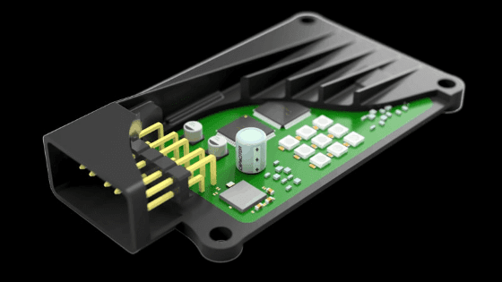
PCB overmolding is an advanced injection molding process where an assembled circuit board (PCBA) is placed into a custom mold and encapsulated with molten rubber or plastic material, forming a robust protective shell. This technology not only provides effective environmental protection but also enhances mechanical stability and improves the product’s aesthetic value.
With the advancement of the Internet of Things (IoT), automotive electronics, and medical devices, the demands for the reliability and durability of electronic products are increasingly high, making PCB overmolding technology ever more critical.
What is PCB Overmolding?
PCB overmolding refers to the process of encapsulating an assembled circuit board using rubber or plastic via an injection molding process. This technique involves placing the PCBA into a custom mold and then filling the cavity with molten material.
After cooling, the material forms a solid protective shell around the board, offering users numerous advantages ranging from electrical insulation to environmental protection.
Custom molds allow users to personalize the final product’s design and shape, while the choice of material determines the protective capabilities and aesthetics. Thus, users can tailor the overmolding to specific applications.
Various types of printed circuit boards can benefit from overmolding, especially those intended for harsh environments, such as in automotive, medical, avionics, and some consumer products.
Types of PCB Overmolding Processes
PCB overmolding is primarily divided into two technical approaches: Low-Pressure Overmolding and High-Pressure Overmolding. These methods differ in their execution, the types of materials used, and the resulting effects, impacting both product functionality and budget.
Low-Pressure Overmolding
The low-pressure process utilizes lower injection temperatures (180-220°C) and pressures (around 100 PSI). This process is mainly suitable for materials with lower viscosity, which require less force to fill the mold.
The lower heat and pressure are suitable for circuit boards populated with precision electronic components, as they prevent damage. Simultaneously, low-pressure molding is more cost-effective, offering an economical solution for high-volume production.
High-Pressure Overmolding
This method involves high material injection pressure (typically starting around 800-2000 PSI, note: 25 PSI mentioned previously is unusually low for high-pressure molding and likely an error; context suggests much higher pressures) and temperature (185-220°C).
Unlike the low-pressure method, it is typically used for viscous materials that require higher pressure to adequately fill the mold cavity.
High-pressure molding is not suitable for PCBs containing fragile components, as the high pressure can damage these parts or even ruin the entire assembly.
Furthermore, high-pressure molding is more expensive, increasing the cost of circuit board protection, and thus has relatively limited application in the electronics field.
Benefits of PCB Overmolding
Enhances IP Rating
During the overmolding process, a material bond forms around the PCB, wires/cables, and connectors. This creates a waterproof seal, preventing dirt, dust, and other debris from entering the electronic components.
Increased Strain Relief
Traditional protective measures like heat shrink, potting, and rear shell connectors do not last as long as overmolded linkages.
Protection Against Shock and Vibration
The overmolding process fills all voids around internal parts, leaving no air gaps that could allow movement. Therefore, overmolding is an optimal method for preventing damage and wear.
Upgrades Low-Cost Components
Overmolding technology creates a robust and weatherproof seal around electrical components. This allows for the use of less expensive parts to build higher-quality electrical assemblies.
Enhanced Aesthetics
Overmolding can be executed in different colors and surface finishes, improving the appearance of electronic devices and making them more appealing to consumers.
Key Advantages of PCB Overmolding
While PCB overmolding adds extra cost, its multiple advantages sufficiently demonstrate the value of this process.
Environmental Protection
Overmolding seals the circuit board within a barrier, providing additional protection. This barrier blocks dust, moisture, chemicals, and more, preventing damage to the board.
In other words, it extends the board’s service life by preventing environmental ingress. The process can typically achieve protection ratings up to IP69, depending on the material type and other characteristics.
Mechanical Protection
Overmolding reduces the likelihood of damage during use in harsh conditions. For instance, the material improves tensile strength and provides stress relief.
This protection is crucial for high-traffic areas of the board, such as around or near connectors. Flexible materials prevent vibration damage, which is vital in specific environments like automotive and industrial applications.
Electrical Insulation
Overmolding materials are non-conductive, effectively isolating the PCB and preventing electrical failures such as arc discharge and short circuits.
The insulation layer also allows for safer handling of the circuit board by users, reducing the risk of electric shock from accidental contact.
Aesthetic and Customization Value
In consumer products and various other applications, the appearance of exposed PCB assemblies is often not appealing. This can not only potentially harm the board but also affect the product’s market acceptance.
Overmolding technology can cover exposed components, thereby enhancing the appearance and making the device more sleek and aesthetically pleasing. Additionally, it allows users to select preferred colors, designs, and shapes, significantly boosting the product’s competitive differentiation.
Common Overmolding Materials and Their Properties
Selecting the appropriate overmolding material is crucial for ensuring the performance of the final product. Materials must be chosen based on their properties and other considerations, such as cost.
Material Classification
PCB overmolding materials mainly include two categories: Thermoplastics and Thermosetting Resins.
- Thermoplastics can be re-melted and reformed. They primarily include TPU (Thermoplastic Polyurethane), TPE (Thermoplastic Elastomer), PVC (Polyvinyl Chloride), Polycarbonate, ABS (Acrylonitrile Butadiene Styrene), and Polyamide (Nylon). These materials soften and melt when heated, hardening again upon cooling, a process that can be repeated.
- Thermosets permanently harden upon heating and cannot be re-melted or reformed. They mainly include Epoxy Resins, Polyurethane, Silicone, and Phenolic Resins. These materials typically offer higher heat resistance and structural stability.
Key Material Qualities
Several key qualities must be considered when selecting an overmolding material:
- Thermal Performance: Suitable for high-temperature environments and high-pressure molding processes.
- Flexibility: Particularly important for wearable devices and applications requiring bending.
- Chemical Resistance: Suitable for harsh environments where contact with chemicals is possible.
- Biocompatibility: Essential for medical electronic devices.
- UV Stability: Applicable for uses where the circuit board is exposed to light.
- Color Compatibility: For aesthetics and product differentiation.
- Optical Clarity: For transparent molds, e.g., those accommodating LED electronics.
Design Considerations and Best Practices for Encapsulation Molding
To ensure the successful implementation of PCB coating, a series of design guidelines and best practices must be followed.
Key Design Considerations
PCB encapsulation molding design requires careful consideration and must adhere to proper design specifications.
The gate location is another critical factor. The gate should be positioned at the thickest section of the TPE wall to ensure good flowability and minimize voids and other defects in the finished product.
To ensure the correct ejection of parts from the tool, the careful construction of the mold is also crucial. This helps reduce defects on the soft surface of the elastomer and guarantees a high-quality final result.
Proper cooling can reduce cycle time and ensure quality.
When manufacturing overmolding molds, it is crucial to consider the flow ratio. For most overmolding applications, the flow ratio should not exceed 150:1L/T. This ensures defect-free filling of the TPE material into the mold.
Best practices
When implementing PCB overmolding, several best practices are worth noting:
Material selection must comply with application requirements: epoxy resin and silicone are suitable for high temperatures, TPE and TPU are suitable for flexibility, while polycarbonate or ABS are suitable for rigidity.
Process control is crucial, and the forming method must be selected to avoid damaging the PCB and its components. Determine the thermal limit of the circuit, ensuring the temperature remains sufficiently low to prevent affecting sensitive devices.
Budget considerations are also essential, as material costs must align with the budget based on specific applications.
If a material capable of controlling circuit board costs is required, an economically efficient solution should be selected.
Design Considerations and Best Practices for Overmolding
Successful implementation of PCB overmolding requires adhering to a series of design guidelines and best practices.
Key Design Considerations
PCB overmolding design requires careful attention and must follow proper design protocols.
- Gate Location is another critical factor. Gates should be positioned at the thickest section of the TPE wall to ensure good flow and reduce voids and other defects in the finished product.
- To ensure proper part ejection from the tool, careful mold construction is crucial. This can reduce marks on the soft surfaces of the elastomer and guarantee a high-quality final result.
- Adequate cooling reduces cycle times and ensures quality.
- When creating overmolding molds, considering the Flow Length to Thickness Ratio (L/T ratio) is very important. For most overmolding applications, this ratio should not exceed 150:1. This ensures the TPE material fills the mold without defects.
Best Practices
When implementing PCB overmolding, several best practices are worth noting:
- Material Selection must align with application requirements: Epoxy and Silicone for high temperatures; TPE and TPU for flexibility; Polycarbonate or ABS for rigidity.
- Process Control is crucial. Select a molding method that does not damage the PCB and its components. Determine the thermal limits of the circuit; temperatures must be low enough not to affect sensitive devices.
- Budget Considerations are essential. Material costs must align with the budget based on the specific application. If a material is needed that controls board cost, choose a cost-effective solution.
How PCB Overmolding Complies with RoHS Regulations
PCB overmolding should utilize materials that comply with RoHS standards. Heavy metals such as Mercury, Lead, Cadmium, and Hexavalent Chromium are strictly prohibited.
Many PCB overmolding materials, such as TPE and TPU, are RoHS compliant. Since these materials do not contain restricted compounds, they are safe for assembling all electronic components.
PCB overmolding manufacturers, besides using RoHS-compliant components, must possess the necessary documentation and testing methods. This involves tracking the materials used and conducting regular tests to ensure ongoing compliance.
Application Areas of PCB Overmolding
PCB overmolding offers multiple advantages and is suitable for various types of electronic equipment and industries:
Automotive Electronics
In the automotive sector, overmolding is used for critical components like sensors, control modules, and lighting systems. The automotive environment places extremely high demands on electronic reliability, and overmolding provides the necessary heat resistance, protection against vibration, and chemical corrosion resistance.
Consumer Products
In the consumer electronics field, products like earbuds, wearable devices, and outdoor gadgets widely adopt overmolding technology. These devices often require slim designs and aesthetic appeal while needing to withstand the impacts and abrasion of daily use.
Medical Devices
The medical field has extremely strict requirements for electronic equipment. Overmolding is used in health monitoring products, diagnostic equipment, implants, etc. These applications typically require biocompatible materials and high reliability to ensure patient safety and proper device operation.
Industrial & LED Applications
In the industrial sector, overmolding is used for rugged sensors, control modules, and other equipment designed for demanding environments. In LED applications, overmolding provides IP protection ratings, enabling LED products to be suitable for outdoor use, such as in lighting, decoration, and signage.
Conclusion
With the rapid development of 5G, IoT, and AI technologies, the demand for high-performance, high-reliability electronic equipment will continue to grow. PCB overmolding technology, as a crucial means of ensuring the stable operation of electronic devices in harsh environments, will see continuous refinement in its processes, and materials science will introduce more high-performance, environmentally friendly materials.
In the future, we can anticipate PCB overmolding playing a key role in more emerging fields—from wearable devices to smart homes, and from smart cities to Industry 4.0. This technology will provide a solid guarantee for the reliability and durability of electronic devices.
Selecting the correct overmolding solution will be one of the key strategies for electronics manufacturers to stand out in the fiercely competitive market.


0 Comments