
The Printed Circuit Board (PCB) is the core of modern electronics, supporting and interconnecting all critical components of an electronic device. Whether in smartphones, computers, or medical equipment, the performance of these devices hinges on effective PCB design and layout.
As electronics evolve, PCBs are becoming increasingly complex, compact, and performance-critical. A successful board layout requires balancing spatial constraints, thermal management, signal integrity, and manufacturability to achieve optimal performance. Meticulous planning during the PCB layout phase lays the foundation for the final product’s reliability and cost-effectiveness.
What is PCB Layout?
Printed Circuit Board layout refers to the physical arrangement of traces and electronic components on a PCB. It translates the electrical schematic into a format that manufacturers can use to fabricate the board. The layout defines the placement of components and how copper traces, pads, and vias interconnect them to create functional pathways. Every decision, from trace width to component orientation, impacts the performance, reliability, and cost of the final product.
A well-considered PCB design and layout ensures signal integrity, minimizes electromagnetic interference (EMI), manages heat effectively, complies with design standards, and enhances manufacturing and assembly efficiency. The quality of the PCB design layout often determines whether a product functions flawlessly or fails prematurely.
Functional Requirements for PCB Component Placement
For optimal PCB performance, components must be positioned to meet the circuit’s functional needs. While placing every component pin for a direct connection to the next pin in the circuit is ideal, this is impractical in high-density layouts. When one circuit’s pins are placed closely, the pins of the next circuit inevitably end up spaced apart. This layout challenge forces designers to make multiple compromises to achieve the best overall PCB performance.
To ensure optimal performance, the first step in creating the best component layout is to plan the placement of functional blocks. These functional partitions help you map out the digital, analog, RF, and power supply areas on the board before starting component placement. The key is to maintain isolation between these areas to prevent noise from one section from affecting another. For the best signal and power integrity in your design, you must also arrange circuit areas judiciously, avoiding the use of split ground planes.
After planning the different circuit areas, you can begin placing components. Here are some general placement guidelines for digital components to keep in mind:
- Place fixed components (e.g., connectors) first, and build the rest of the placement around them.
- Do not allow components from one area of the circuit to encroach upon another area—except for transition components like analog-to-digital converters.
- When laying out dense circuit areas, remember to leave space in inner areas for escape routing and bus routing. Do not block routing channels.
- Remember that vias used for escape and bus routing can obstruct signal return paths on reference planes, so plan ahead to maintain clear return paths.
- Place components for high-speed signals close together so that routing can follow the signal path in the schematic. These connections need to be short and direct.
When placing the analog and power sections in your design, you should follow the same general guidelines. To achieve good power integrity, power components must also adhere to some additional requirements:
- High-speed components with high power consumption (e.g., processor devices) require numerous decoupling capacitors connected to their power pins. This can be a significant challenge for devices with high pin counts in BGA packages, but these capacitors must be placed as close as possible to their pins to control ground bounce and other power integrity issues.
- Place power components as close together as possible. This keeps the traces between pins short and wide, which is crucial for reducing inductance.
- Keep power components on the same layer of the board to eliminate the need for vias, which also introduce unwanted inductance.
Component placement should also consider the heat they generate during operation. Components that run hot, like processors, should be placed near the center of the design for better heat dissipation across the board. Individual power supplies should not be placed adjacent to each other. Also, pay attention to the board’s airflow to avoid obstructing heat dissipation. This may require relocating taller components that block airflow. Furthermore, during placement, allocate space for heat sinks and other thermal management devices and strategies.
With these practical PCB component layout guidelines, you might think it’s sufficient for any designer. But there is more—we now need to evaluate the component layout from a manufacturing perspective.
Fundamental Steps in PCB Layout Design
PCB layout design is a systematic process where decisions at each stage impact downstream performance, manufacturability, and cost. These foundational steps set the stage for a reliable and efficient design:
1. Goal Definition and Conceptualization
The process begins by clearly defining the PCB’s purpose. By establishing design goals and conducting extensive research, you can determine the requirements the designer needs to meet. These requirements include the board’s core functions, key features, the number and type of required connections to other circuits, and the approximate size. The board’s location within the final product and its operating environment (including temperature range) are also important considerations.
A board-level block diagram maps the PCB’s high-level structure, including its final dimensions. In some cases, Computer-Aided Design (CAD) software can be used to create a better, more compact design, which is crucial in the modern PCB layout workflow. These tools enable engineers to create precise schematics, design complex board layouts, manage component libraries, verify designs through simulation, and generate manufacturing files required for production.
The block diagram defines how the board’s sections relate spatially and electrically, outlining areas for specific functions. During conceptualization, grouping related components helps minimize trace lengths and improve signal integrity.
2. Schematic Creation
Following conceptualization and requirement definition, the next step is translating ideas into a detailed circuit schematic. This schematic serves as the electrical, mechanical, and physical blueprint of the board, showing all components, their interconnections, and technical specifications like voltage ratings and part numbers.
Here, the engineer also creates the Bill of Materials (BOM), listing all components required for production. A well-structured schematic simplifies the layout phase and facilitates future revisions and troubleshooting.
3. Component Selection and Placement
The strategic placement of components is one of the most critical phases in PCB layout design. Engineers must carefully position each component based on functionality, accessibility, thermal management, and manufacturability. Precise placement directly impacts routing efficiency, signal integrity, thermal control, and board reliability. Designers often iterate on the placement multiple times to achieve an optimal layout.
4. PCB Routing and Schematic Draft Finalization
After components are placed, the next step is routing the electrical connections. Initial routing involves defining trace paths to ensure minimal signal attenuation and efficient power delivery. Early routing decisions often reveal layout challenges, potentially requiring fine-tuning of the placement or board structure.
After the initial routing phase is complete, engineers perform additional steps, including:
- Simulation
- Requirement Verification
- Engineering Review
These steps are repeated as necessary. The engineer then finalizes the draft and begins prototyping.
5. Testing and Verification
The final step is performing a series of checks to ensure the layout meets all electrical testing requirements and functions as intended. These tests include continuity, flying probe testing, adjacency checks, and resistance and capacitance tests. Any issues identified now are far easier and less costly to correct than after production.
Requirement verification and engineering reviews are repeated as needed. The design is only complete after passing all tests relevant to your requirements, finalizing the schematic, and commencing production.
PCB Layout Process and Specific Guidelines
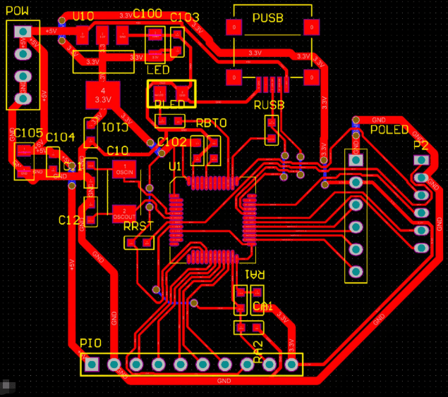
Step 1: Fixed Component Placement
- Connectors: Such as power jacks, USB, Ethernet ports, etc., must be placed strictly according to mechanical constraints, typically along the board edge.
- Indicators, Switches: Positioned in locations easily visible and accessible to the user.
- Large Components: Such as heat sinks and transformers. Pay attention to their height and placement to avoid interference with the enclosure or other components.
- Mounting Holes: Placed first, with sufficient keep-out areas around them.
Step 2: Core IC and Critical Circuit Module Placement
- Main Control Chips (MCU/CPU/FPGA): Placed near the center of the board or close to their primary functional modules. Consider heat dissipation; provide thermal vias underneath if necessary.
- Memory (DDR/SDRAM):
- Placed close to the main controller to minimize the length of data/address/clock lines.
- High-speed buses like DDR require strict topology and length matching; plan the routing space during the layout phase.
- Power Modules:
- Shortest Power Path Principle: Place power chips, inductors, and input/output capacitors compactly to form the smallest current loop, reducing parasitic inductance and EMI.
- Sequence: Input capacitor -> Power chip -> Inductor -> Output capacitor. Capacitors should be as close as possible to the chip pins.
Step 3: Functional Modularization and Collaborative Layout
- Zoning/Layout by Area: Divide the board into analog, digital, RF, and power areas.
- Analog/Digital Separation: Use physical separation (e.g., routing slots) or ground plane splits to reduce digital noise interference with analog circuits.
- High-Frequency/RF Circuit Isolation: Shield using cans or dedicated areas, with proper impedance control.
- Layout Based on Signal Flow: Ensure the signal path is as smooth and direct as possible, avoiding detours and backtracking.
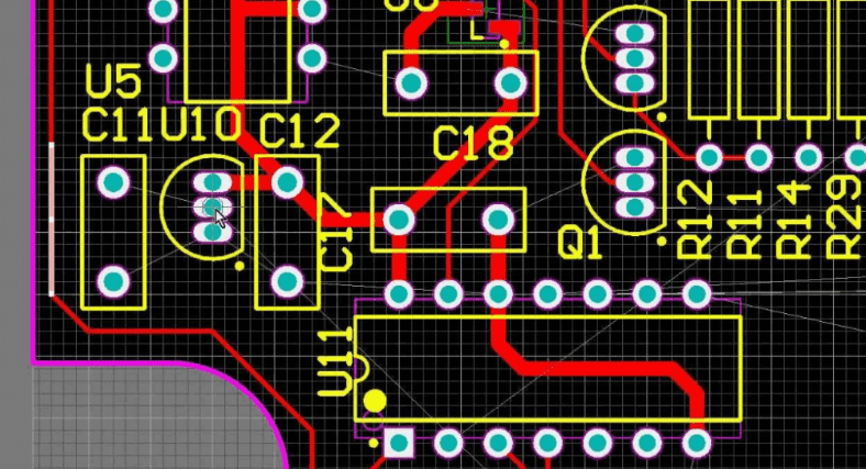
Step 4: Decoupling Capacitor Placement
This is critical for ensuring power integrity.
- Priority to Small Capacitors (0.1µF, 0.01µF): The smallest decoupling capacitors (for high-frequency noise) must be placed closest to the IC’s power/ground pins.
- Larger Capacitors (10µF) Next: Used for low-frequency decoupling and bulk capacitance, can be placed slightly farther but still within the same region.
- Direct Via Connection to Power/Ground Planes: The capacitor’s vias should be placed directly on the pad or immediately adjacent, connecting directly to the inner power and ground planes through the via, rather than through long traces.
Step 5: Detail Adjustment and Optimization
- Spacing Check: Ensure sufficient clearance between components to meet soldering process requirements (e.g., preventing solder bridges).
- Silkscreen Placement: Position reference designators, version numbers, polarity markers, etc., in clear, non-overlapping locations to facilitate soldering and debugging.
- Thermal Considerations: Allocate sufficient copper area and space for components with high heat dissipation (e.g., LDOs, power devices). Add thermal vias or heat sinks if necessary.
Special Considerations for High-Frequency and Thermally Sensitive Components
Handling High-Frequency Components
When dealing with components operating at high speeds, such as Wi-Fi chips or high-speed processors, it is essential to ensure they are kept away from objects that might interfere with the signal. Specific methods include:
- Isolate them from noise-emitting objects (e.g., motors, power supplies).
- Use short paths for signals to keep them strong and clear.
- Place shielding around them to block any unwanted signals.
Intelligently Handling Thermally Sensitive Components
For components that are less tolerant of excessive heat, such as certain computer chips or voltage regulators, careful placement is mandatory. Specific methods include:
- Keep them away from heat-generating objects, such as large resistors or power components.
- Ensure airflow can circulate around them to prevent overheating.
- Employ special techniques, such as additional copper pours or heat sinks, to help them stay cool.
- Consider their orientation to promote proper cooling.
4 PCB Routing Best Practices
Routing and signal management are crucial in PCB layout design. Employing thoughtful PCB routing techniques helps maintain good signal quality and avoids unnecessary issues during manufacturing or field operation.
1. Minimize Signal Interference and Crosstalk
To preserve signal integrity, it is vital to minimize interference between traces and ensure clear signal paths. Here are some techniques you can employ:
- Provide Ample Spacing: Leaving sufficient space between signal lines prevents electromagnetic coupling and minimizes crosstalk, thereby enhancing overall signal clarity.
- Avoid Parallel Traces: Avoid routing signal traces parallel to each other to reduce mutual inductance and the potential for signal interference. When crossing is necessary, route traces at right angles to minimize coupling.
2. Consider Power, Ground, and Signal Traces
Thoughtful planning of power and ground planes, along with signal trace design, enhances mechanical stability and electrical performance. Here are some effective PCB routing guidelines you can implement:
- Use Robust Power and Ground Planes: Centralized and symmetrical power and ground planes reduce board warping and minimize electromagnetic emissions. Internal planes provide low-impedance return paths for signals. Large ground planes also shield the circuit and prevent interference.
- Ensure Appropriate Trace Widths: Sizing traces according to the required current load helps prevent PCB overheating, excessive resistance, and signal degradation. Ensure traces are analyzed to avoid unintentionally forming antennas resonant at the circuit’s operating frequencies.
- Use Multiple Vias for High-Current Paths: When transitioning between layers, distribute high-current loads across multiple vias. This technique lowers resistance and improves thermal conductivity.
3. Control High-Speed Signal Routing and Impedance
High-speed signals are sensitive and require precise routing and impedance management to maintain signal quality.
- Route High-Speed Signals over a Solid Ground Plane: Always route high-speed traces directly over a continuous ground plane to maintain consistent impedance and signal fidelity.
- Use 135-Degree Trace Bends: Avoid 90-degree trace bends, as they can cause signal reflection and attenuation, especially at higher frequencies. 135-degree bends provide a smoother signal flow.
4. Strategically Place Components and Traces
Positioning critical components and routing traces intelligently enhances signal flow and board performance, even if compromises are sometimes necessary.
- Strategic Component Placement: Place critical components like high-speed Integrated Circuits (ICs) or power components in locations that allow for the shortest trace lengths and avoid thermal interference.
- Route Signals According to Flow: Ensure signals flow in the same direction from input to output, keeping trace lengths short and direct for optimal performance.
Summary
PCB layout is an art of trade-offs and compromise, requiring a balance between performance, cost, manufacturability, and time. By following these guidelines and best practices, you can systematically create high-quality, highly reliable PCB designs.


0 Comments