
Introduction
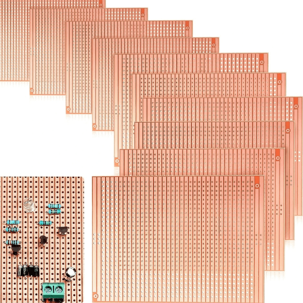
A blank PCB, often referred to as a bare board or printed circuit board, is an insulating substrate with pre-etched conductive copper traces (circuitry) and drilled holes for mounting electronic components. However, it has not yet been populated with any electronic components (such as resistors, capacitors, chips, etc.).
Think of it as the foundation of a city, with planned roads and reserved building plots, but without any constructed houses, shops, or infrastructure.
A blank PCB, also known as a bare PCB or empty PCB, is an electronic board laminated from epoxy fiberglass, copper foil, and PCB ink.
What is a Blank PCB?
A blank PCB initially consists of a non-conductive plane, typically made from composite materials like FR-4. A conductive copper layer is then patterned onto it, usually through a process called photolithography. This patterned copper layer forms the interconnections between components according to the circuit diagram’s requirements.
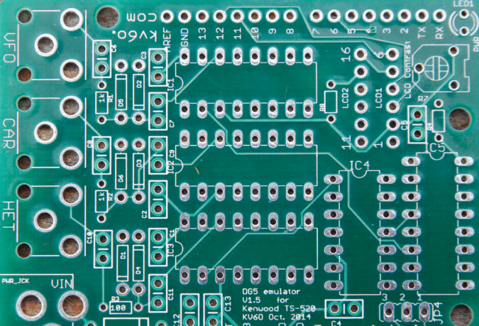
Before components like ICs, resistors, or capacitors are soldered onto it, the PCB is referred to as a “blank” or “bare” board. A blank PCB can range from a basic single-sided board with copper on one side only, to a complex multilayer board containing over 20 conductive layers.
Also Known as a Bare PCB
Blank PCBs are also called bare printed circuit boards because they have not yet been fitted with any electronic components. These substrates consist solely of an insulating base and conductive copper lines, without any connected peripherals or devices.
The terms “blank PCB” and “bare PCB” are often used interchangeably. Other names, such as substrate, empty board, or unfinished board, are also sometimes used. However, in most manufacturing and design documentation, these unfinished boards are referred to as blank PCBs or bare PCBs.
Circuit Board Foundation
Blank PCB boards serve as the assembly platform for all circuit components, such as processors, capacitors, switches, and chips. The layered copper interconnects provide conductive paths between different components, enabling the efficient transmission of power and signals according to the intended circuit function.
Higher-end blank boards may also integrate contacts and communication interfaces, like USB ports or display connectors, during the manufacturing process. This facilitates integration during PCB assembly or downstream device manufacturing, based on requirements. Understanding the performance and manufacturing processes of blank PCBs aids in better electronic product development.
Key Components of a Blank PCB
A typical blank PCB generally consists of the following parts:
- Substrate:
- This is the main body of the PCB, typically made of insulating material, most commonly glass fiber epoxy resin. For flexible circuit boards, flexible materials like polyimide are used.
- It provides structural support and electrical insulation.
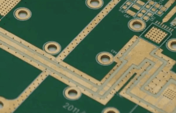
- Copper Layer:
- This is one or more thin layers of copper foil laminated onto the substrate. Unwanted copper is chemically etched away, leaving behind the circuit traces that connect various component points.
- Based on the number of copper layers, PCBs are classified as single-sided, double-sided, or multilayer boards.
- Solder Mask:
- This is a layer of green (or other colors like blue, red, black) paint covering the copper traces.
- Its purpose is to prevent oxidation of the copper and avoid solder bridges (short circuits) during the soldering process.
- Silkscreen Layer:
- This consists of white (or other light colors) text and symbols printed on top of the solder mask.
- It is used to label component designators (e.g., R1, C2), polarity, chip orientation, etc., facilitating assembly and debugging for engineers and technicians.
- Pads:
- These are exposed annular ring areas of copper on the PCB, intentionally left uncovered by the solder mask for soldering component leads.
- They are the points where components make electrical and physical connections to the board.
- Vias:
- On double-sided or multilayer boards, these are small metallized holes used to connect copper traces on different layers.
Types of Blank Printed Circuit Boards
FR4 PCB
FR4 PCBs are the most common type of blank PCB. “FR4” does not refer to a specific material but denotes a Flame Retardant等级 4. Essentially, an FR4 PCB is an epoxy fiberglass PCB with a flame retardant等级 of 4. The prepreg layers between copper layers are also epoxy fiberglass but are partially cured.
FR4 blank PCBs are easy to manufacture. When obtaining online PCB quotes, you will find FR4 PCBs are more affordable than other types with the same layer count and circuit complexity.
Metal Core PCB (MCPCB)
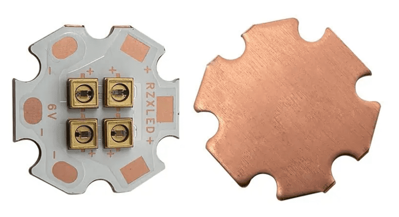
Metal Core PCBs include Aluminum Core PCBs and Copper Core PCBs. Metal PCB substrates have significantly better thermal conductivity than FR4 cores. MCPCBs are primarily used in LED lighting and other power applications.
All Metal Core Printed Circuit Boards (MCPCBs) use a dielectric layer to isolate the metal core from the copper circuit layer. In fact, the dielectric is the primary factor determining the thermal conductivity of an MCPCB. For copper core PCBs, manufacturers like PCBONLINE can achieve thermal-electrical isolation, with PCB thermal conductivity reaching up to 398 W/mK.
Flexible PCB and Rigid-Flex PCB
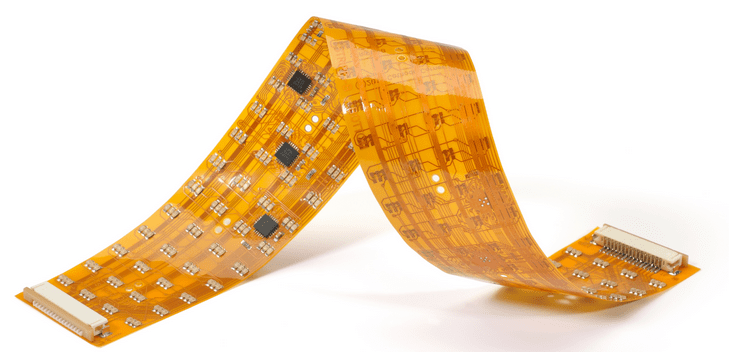
Flexible PCBs and Rigid-Flex PCBs are bendable blank PCBs based on PI or PET. Rigid-Flex PCBs are a special type of flexible PCB where the flexible parts are laminated with FR4 PCB sections.
The copper foil used in flexible PCBs is RA (Rolled Annealed) copper or ED (Electrodeposited) copper, while Rigid-Flex PCBs typically use only RA copper. An adhesive layer exists between the PI film and the copper foil.
High-Frequency PCB
High-Frequency PCBs are also high-speed RF microwave PCBs. They are blank PCBs based on PTFE, used for transmitting and receiving high-frequency signals. High-Frequency PCBs find applications in antennas, radar, collision avoidance systems, GPS, smartphones, missile systems, etc.
The thermal expansion and contraction (CTE) of PTFE material can significantly impact the performance of high-frequency PCBs; minimal thermal expansion is desired. Manufacturer PCBONLINE possesses core technologies to minimize the thermal expansion and contraction of high-frequency PCBs. You can contact PCBONLINE for high-frequency PCB information.
AlN PCB and Alumina PCB
Aluminum Nitride (AlN) and Alumina are two ceramic materials with good thermal conductivity. AlN has a relatively low Coefficient of Thermal Expansion (CTE), close to that of semiconductors, making AlN PCBs currently an excellent PCB choice for ICs.
AlN PCBs and Alumina PCBs can be used in high-power LED lighting, laser electronics, automotive sensors, etc.
Besides ceramic PCBs, glass substrate PCBs can also be considered, as they offer good thermal expansion properties and are transparent.
Benefits of Using Blank PCBs
Compared to assembling circuits on perforated boards or using breadboards for prototyping, blank PCB manufacturing offers significant advantages. These benefits make blank PCBs an indispensable part of modern electronic design and production.
Flexibility and Customizability for Diverse Designs
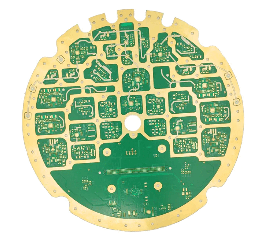
Blank circuit boards offer great flexibility as they can be manufactured according to different circuit requirements. The blank PCB manufacturing process can produce boards ranging from single-sided to over 32 conductive layers, enabling cost-effective integration of complex circuits.
They also face no inherent restrictions in size or shape during design or manufacturing. Rectangular blank PCBs are common, but circular, triangular, or irregularly shaped boards can also be produced based on mechanical requirements. This design flexibility allows PCBs to be seamlessly fitted into various devices and enclosures.
Manufacturing blank PCB boards, as opposed to manual circuit assembly, also provides extensive customization capabilities. This allows for the integration of precise circuit paths, interconnect densities, heat sinks, and interfaces as required.
Cost Savings
Producing blank printed circuit boards, especially in large volumes, offers substantial cost savings over manual methods. Economies of scale combined with efficient manufacturing processes reduce overall costs.
As fixed infrastructure and labor costs are amortized over production volumes, the per-unit cost of each blank PCB decreases. This enables companies to maintain profit margins while selling devices containing PCBs at lower prices. The saved costs can also be allocated to offering more product features, enhancing competitiveness.
Faster Time-to-Market
Blank PCB manufacturing also accelerates the time-to-market for electronic products. Instead of manually designing and assembling multiple prototypes, most design verification and testing can be performed on manufactured blank boards.
Potential issues with the circuit or board layout can be identified within just a few iterations before final production begins. This avoids costly delays due to prototyping problems. Consequently, blank PCBs help significantly shorten the product development lifecycle.
Support for Prototyping and Testing
Manufacturing blank PCB boards provides an effective platform for testing circuit designs through prototype iterations. Multiple design concepts can be rapidly iterated on pre-fabricated blank boards without manual point-to-point wiring.
This prototyping process validates circuit functionality, thermal performance, signal integrity, and potential interference issues. Any problems identified during prototyping on blank boards can be rectified before final design freeze. This ensures the PCB circuit and layout function as intended post-production.
Therefore, blank boards can significantly enhance development efficiency through iterative prototyping. They facilitate early detection of design flaws, saving considerable time and development costs.
Manufacturing Process of Blank PCBs
The manufacturing process for blank PCBs is a highly precise and complex multi-step procedure involving fields such as photochemistry, electrochemistry, and mechanical processing. The process is detailed below.
The entire process can be summarized into three main stages: Pre-Production -> Core Pattern Formation & Processing -> Post-Processing & Testing.
Stage 1: Pre-Production
- Step 1: Design & File Output
- Activity: After completing the PCB layout design using EDA software, the engineer generates a set of standard manufacturing files, primarily Gerber files (describing layer patterns), drill files (describing hole locations and sizes), and aperture files.
- Purpose: These files serve as the “construction blueprint” for the PCB factory; all manufacturing steps are based on them.
- Step 2: Material Preparation – Copper-Clad Laminate
- Activity: Preparation of the base material – the Copper-Clad Laminate (CCL). It typically consists of an insulating substrate with a copper foil layer laminated onto its surface.
- Purpose: Provides the structural support for the circuit and the foundation for conductive pathways.
Stage 2: Core Pattern Formation & Processing
This is the most critical stage in manufacturing, aiming to “draw” the designed circuit pattern.
- Step 3: Pattern Transfer
- Goal: Precisely replicate the circuit pattern from the design files onto the copper-clad laminate.
- Two primary methods exist:
- Photolithography:
- Photoresist Coating: A layer of UV-sensitive photoresist is applied to the cleaned copper-clad laminate.
- Exposure: A film with the circuit pattern (produced from Gerber files) is placed tightly against the photoresist-coated board and exposed to UV light. The photoresist areas under the transparent parts of the film undergo a chemical change (for positive photoresist).
- Development: The board is rinsed with a chemical solution that dissolves the exposed (or unexposed, depending on photoresist type) areas, revealing the underlying copper foil.
- Printing & Etching: Another common method, particularly suitable for prototypes and small batches.
- Photolithography:
- Step 4: Etching
- Activity: The board, after pattern transfer, is placed into an etching machine and subjected to a strong alkaline or acidic chemical solution (e.g., ferric chloride, ammonium hydroxide).
- Purpose: To corrode away all the copper foil not protected by the photoresist, leaving behind the protected copper that forms the final circuit traces.
- Step 5: Stripping & Cleaning
- Activity: Another chemical solution is used to completely remove the photoresist layer protecting the copper traces.
- Purpose: To reveal the now-formed, shiny copper circuitry and thoroughly clean the board for subsequent steps.
Stage 3: Interlayer Connection & Protection
- Step 6: Drilling
- Activity: Use high-speed CNC drilling machines, controlled by drill files, to precisely drill holes in the board for:
- Component Holes: For inserting component leads.
- Vias: For connecting traces on different layers.
- Mounting Holes: For mechanical fastening.
- Purpose: To provide channels for component mounting and interlayer electrical connections.
- Activity: Use high-speed CNC drilling machines, controlled by drill files, to precisely drill holes in the board for:
- Step 7: Hole Metallization (Plating)
- Activity: This is a core step for manufacturing double-sided and multilayer boards. The walls of the drilled holes are insulating and need to be made conductive.
- Electroless Copper Deposition: Through a series of complex chemical treatments, a thin layer of chemical copper is deposited on the hole walls, making them initially conductive.
- Electroplating: An electroplating process is used to thicken the copper layer on top of the chemical copper, ensuring conductivity and reliability of the hole walls.
- Purpose: To achieve electrical connections between different conductive layers.
- Activity: This is a core step for manufacturing double-sided and multilayer boards. The walls of the drilled holes are insulating and need to be made conductive.
Stage 4: Post-Processing & Protection
- Step 8: Solder Mask Application
- Activity:
- Solder mask ink, typically green (but also blue, red, black, etc.), is applied over the entire board surface.
- Using a process similar to pattern transfer (exposure and development), only the pads intended for soldering are left exposed; all other areas are covered by the solder mask.
- Purpose:
- Prevent Solder Bridges: Avoids solder shorting to adjacent traces during soldering.
- Protect Traces: Prevents oxidation and damage to copper traces during subsequent use.
- Insulation: Improves electrical safety.
- Activity:
- Step 9: Silkscreen Printing
- Activity: Screen printing technology is used to print white (or other light colors) text and symbols (e.g., component designators, polarity, company logo) onto the solder mask.
- Purpose: To provide clear identification for subsequent component assembly, testing, and repair.
- Step 10: Surface Finish
- Activity: A special treatment is applied to the exposed pads to prevent oxidation and ensure good solderability. Common processes include:
- HASL: Low cost, good solderability, but uneven surface.
- ENIG: Flat surface, strong oxidation resistance, suitable for fine-pitch pads and wire bonding.
- Immersion Tin/Silver: Provides good flatness and solderability.
- OSP: Forms an organic protective film on the copper surface; low cost but shorter shelf life.
- Purpose: To ensure the pads remain “fresh” and easy to solder when they reach the assembly factory.
- Activity: A special treatment is applied to the exposed pads to prevent oxidation and ensure good solderability. Common processes include:
Stage 5: Finalization & Inspection
- Step 11: Panelization/Separation (Depanelization)
- Activity: Use V-scoring machines or CNC routing machines to cut the entire production panel into the final shapes and sizes required by the customer.
- Purpose: To obtain the final outline of individual PCBs.
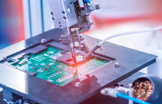
- Step 12: Electrical Testing
- Activity:
- Flying Probe Test: Uses multiple movable probes to contact pads and test circuit continuity (opens/shorts). Suitable for small batches.
- Fixture Test (Bed of Nails): A dedicated test fixture is created to test all networks of the entire board simultaneously. Suitable for large volumes.
- Purpose: To 100% ensure the PCB is free from opens (should be connected but aren’t) and shorts (shouldn’t be connected but are), complying with design specifications.
- Activity:
- Step 13: Final Inspection & Packaging
- Activity: A final visual inspection is performed to confirm dimensions, hole positions, silkscreen, etc., meet requirements. Then, vacuum packaging is used to prevent moisture absorption and physical damage.
- Purpose: To deliver qualified products safely to the customer.
Summary Process Flow
Design -> Output Gerber -> Prepare CCL -> Pattern Transfer -> Etching -> Stripping -> Drilling -> Hole Plating -> Solder Mask -> Silkscreen -> Surface Finish -> Profiling -> Testing -> Inspection & Packaging.
Best Practices for Handling, Storing, and Shelf Life of Blank PCBs
Although blank PCBs may appear robust, they are sensitive components whose performance can degrade if handled or stored improperly. Moisture absorption, contamination, and Electrostatic Discharge (ESD) are key concerns affecting manufacturability and final product reliability.
Many dielectric materials used in blank PCBs, especially epoxy-based resins like FR-4, are hygroscopic, meaning they absorb moisture from the environment. Excessive moisture absorption can lead to several issues:
- Degraded Electrical Performance: Moisture can increase the substrate’s dielectric constant (Dk) and dissipation factor (Df), potentially affecting impedance control and signal integrity in high-speed circuits. Moisture also reduces insulation resistance, increasing the risk of leakage currents.
- Delamination and “Popcorning”: During high-temperature assembly processes like reflow soldering, trapped moisture can rapidly vaporize, creating internal pressure that leads to delamination (layer separation), blistering, or “popcorning” (internal voids).
- Reduced Tg: Absorbed moisture can lower the resin’s Glass Transition Temperature, making the material more prone to deformation at elevated temperatures.
- Impact on Solderability: Oxidation or contamination on copper surfaces, combined with moisture, can impair solderability.
IPC-1601A (Printed Board Handling and Storage Guidelines) outlines procedures for moisture-sensitive PCBs, including pre-assembly baking protocols and Moisture Sensitivity Level (MSL) classification.
Guidelines for Optimal Storage and Maintaining PCB Integrity
Proper storage is crucial for preserving blank PCB quality and extending shelf life:
- Environment: Store blank PCBs in a stable, dry, temperature-controlled environment, ideally between 15°C and 30°C, with relative humidity (RH) between 40% and 65%. Avoid storage in damp areas and locations with significant temperature fluctuations.
- Packaging: For moisture-sensitive materials or long-term storage, blank PCBs should be vacuum-sealed in Moisture Barrier Bags (MBB) with desiccant packs and Humidity Indicator Cards (HIC) included. Anti-static bags or containers should be used to prevent ESD damage, especially for boards with fine features. For Immersion Silver finishes, sulfur-free and pH-neutral packaging materials are recommended to prevent tarnishing.
- Handling: Minimize direct physical contact with the blank PCB surfaces. Always handle boards by their edges, wearing clean, lint-free, anti-static gloves. Avoid using hand lotions or other products that might transfer contaminants. Use appropriate racks, trays, or protective bags when transporting boards within facilities. Workstations should be kept clean to prevent Foreign Object Debris (FOD) contamination.
- Shelf Life: The usable shelf life of a blank PCB depends heavily on its surface finish and storage conditions.
- OSP-coated boards typically have a shorter shelf life (e.g., 6-12 months) and are more sensitive to handling and atmospheric conditions.
- Metallic surface finishes, such as ENIG, Immersion Tin, or HASL, generally offer a longer shelf life (e.g., 12 months or more) if stored properly.
- Proper vacuum packaging and controlled storage environments are crucial for maximizing shelf life and ensuring good solderability when the blank PCB is ultimately used. Regular inspection of stored boards and their packaging is advised.
A blank PCB is not just a passive laminate; it is a precision substrate whose performance depends on stringent environmental control. Treating PCBs with the same care as sensitive components is essential for ensuring solderability, electrical stability, and final product reliability. Robust handling and storage protocols, compliant with IPC guidelines, protect your investment from damage even before the first component is mounted.
Applications of Blank PCBs
Today, versatile blank PCB manufacturing capabilities enable their widespread use across various electronic products and sectors, including:
- Consumer Electronics
From smartphones and laptops to tablets, home appliances, and gaming consoles, printed circuit boards permeate every facet of consumer electronics. High-volume production, compact form factors, and consistent quality levels make this a leading PCB application today. - Industrial Electronics
Machinery controls, robotics, power conversion, and monitoring systems used in factories often employ PCBs customized for the demands. Withstanding higher temperatures and vibrations, and possessing noise immunity, often requires enhanced manufacturing processes. - Automotive Electronics
Modern connected cars may contain dozens to over a hundred custom blank PCBs tailored for efficiency, safety, and comfort applications. Stringent quality requirements, given the harsh under-hood environment and long-life demands, necessitate specialized PCB manufacturing. - Aerospace and Defense:
Ruggedized avionics systems and navigation electronics in aerospace applications use specially processed circuit boards capable of reliably withstanding extreme altitudes and temperature variations over decades. Defense electronics similarly require specialized blank PCBs conforming to strict specifications. - Medical Devices
Life-critical medical instruments and implantable devices (like pacemakers) have rigorous electronic performance requirements coupled with demanding size, biocompatibility, and reliability needs, which custom blank PCB manufacturing is designed to meet. - IoT and Wearable Devices
The burgeoning IoT and wearable device category also increasingly adopts advanced PCB technologies to enhance functionality while minimizing size and cost. This broad application will further drive PCB innovation across all application categories in the future.
Summary
In simple terms, a blank PCB is the “carrier” and “connection platform” for electronic circuits. It possesses no inherent function itself but provides a correct, reliable, and efficient foundation for the mounting and interconnection of all electronic components. Without PCBs, it would be nearly impossible to manufacture the complex, compact, and reliable electronic devices we have today.
A Vivid Analogy:
- A Blank PCB is like a musical score, with the staff and notes written on it, but not yet played.
- A Populated PCB (with soldered components) is like a live performance by an orchestra following the score; only then does the music (circuit function) truly come to life.


0 Comments