
Circuit symbols play a crucial role in electrical and electronic diagrams, representing complex circuits and components in a standardized and simplified manner. These symbols are vital for engineers, electricians, and technicians to understand circuit functionality, often without referring to extensive documentation. Their universal recognition ensures consistent interpretation across different languages and regions, facilitating education and training.
Circuit diagrams consist of various components such as switches, capacitors, resistors, and batteries, interconnected via networks or paths. Each component possesses its unique symbol and characteristics. Understanding how components function is fundamental to effective circuit design and analysis. Knowledge of the properties of resistors, capacitors, and transistors enables engineers to predict interactions between components, achieve desired outcomes, and troubleshoot issues.
How are Circuit Symbols Composed into Circuit Diagrams?
Electronic circuit symbols are concise graphical representations or pictograms used to depict various components within a schematic diagram. In such diagrams, electrical components typically have two or more terminals for connections. Basic electrical and electronic symbols include ground electrodes, batteries, and resistors. These symbols aid in representing even the most complex circuits. With these fundamental symbols, anyone can draft a circuit diagram. For instance, a basic circuit comprises a battery, a switch, and a light bulb connected in a closed loop.
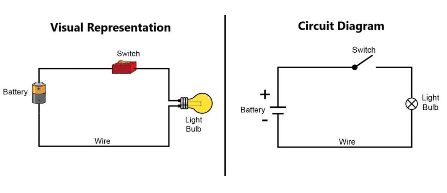
While the same circuit can be represented in multiple formats, visual representation is often more intuitive. However, visual complexity increases with the number of components. Understanding electronic symbols is crucial when undertaking projects involving circuit construction or PCB design. Schematic layout is the first step in PCB design, and progress on such projects can be very difficult without comprehending the symbols used.
Representing Circuits with Symbols and Text
Often, defining anything with specific words is sufficient, but circuit diagrams offer their own advantages. By utilizing symbolic formats, circuit diagrams become clear at a glance. Representing a circuit with text is a straightforward process. For example, the circuit shown above can be described as “a battery connected in series with a switch and a light bulb.” This is easy to understand; however, as circuit diagrams become larger and more complex, using circuit diagrams and symbols becomes necessary. This helps people analyze circuits quickly and understand what is happening. In short, electronic symbols simplify our understanding of circuits, saving time and making things easier.
Advantages of Circuit Symbols
The precise meaning of a symbol is composed of dots, lines, letters, letter spacing, shading, and numbers. Familiarity with the basic structure of various symbols is essential to understand a circuit and the meaning conveyed by its corresponding symbols. The primary advantages of using symbols are as follows:
- Reduces Confusion in Production: By using a defined set of electrical symbols, it is impossible to assign different symbols to similar components.
- Reduces Rework: Developing and using a single, standardized set of electrical symbols eliminates unnecessary and redundant schematic rework.
- Improves Electrical and Mechanical Communication: Using standardized electrical symbols reduces misunderstandings between MCAD and ECAD team members. The connection between 2D symbols and 3D model parts ensures consistent understanding for everyone.
- Saves Time: Standardized electrical symbols save time not only by reducing rework and misunderstandings but also through increased efficiency.
Physics Behind Symbol Design
Symbols are used to denote electrical/electronic components. As mentioned, understanding how components work is very important, and this is the origin of different symbol design philosophies. Each symbol explains the fundamental physics behind the actual component. Most symbol designs are based on different national and international standards, such as IEC, JIC, ANSI, IEEE standards, etc. Although electrical symbols are standardized, variations can exist between different engineering disciplines based on tradition.
Examples Explaining Circuit Physics: Most circuit symbols include switches and batteries, whose symbols are shown below:
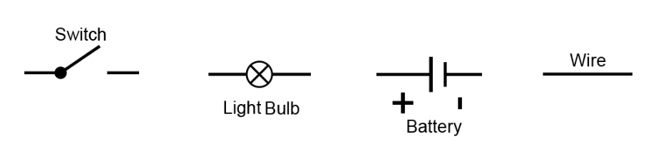
- Switch: The switch symbol above represents making and breaking circuit connections within a circuit, making this symbol universally applicable.
- Light Bulb: The bulb itself possesses resistance and emits light when heated. The cross mark at the light source in the diagram indicates that the light originates from a resistive source.
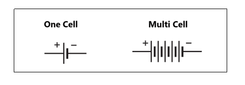
- Battery: It is a source of energy composed of cells, containing chemical electrolyte internally that provides polarity. The cells in the battery symbol are represented by two parallel lines of unequal length, with the positive and negative terminals marked on them.
- Wire: It is simply a connecting conductor between two devices with very low resistance, so it is represented by a straight line for the connection.
There are other more complex symbols that are not easily interpreted without knowledge of the component.
Circuit Diagram Symbol List and Their Design Physics
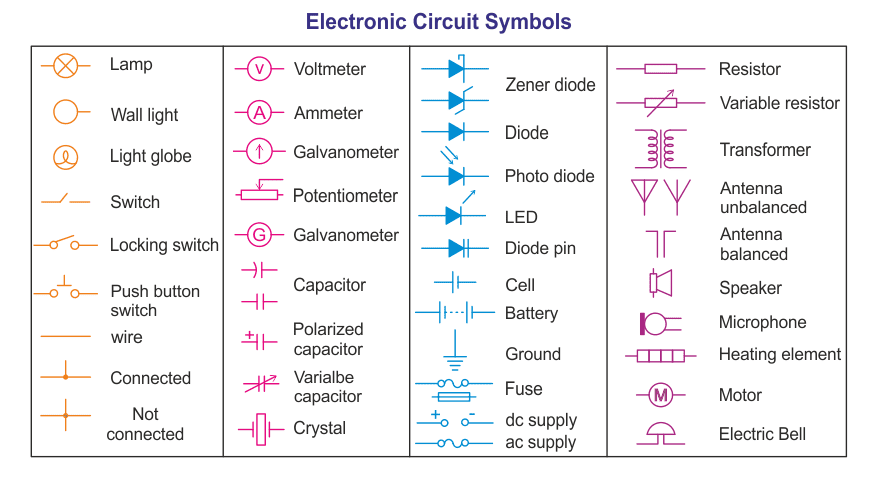
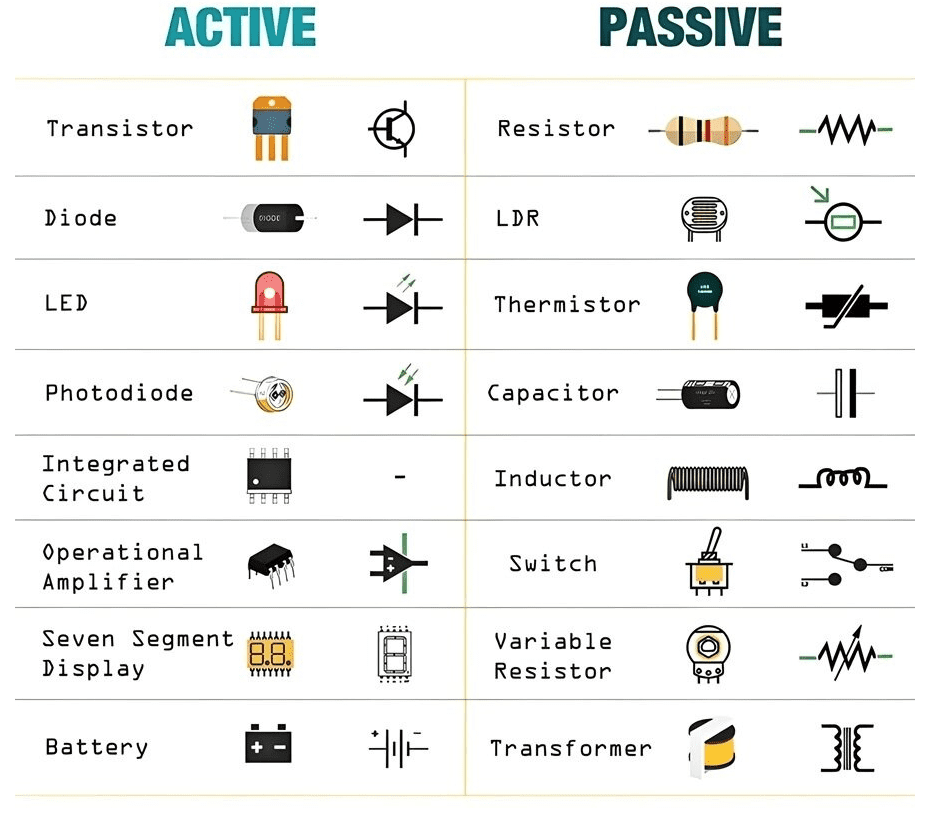
Circuit diagrams are used to visually depict the symbols used in electronic circuits. Each circuit utilizes standardized symbols to represent its individual parts. Representing basic electrical devices requires the use of a variety of electronic circuit symbols. Each electrical device or component used in a circuit has a circuit symbol, such as passive components (resistors, capacitors, inductors), active components (diodes, transistors, amplifiers, transformers), measuring devices, and logic gates. Below are the most commonly used electronic component symbols and the design physics behind them:
Passive Components:
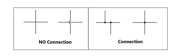
- Wire: Used to connect different components, hence represented by a straight line. Two crossing wires may or may not be connected. If not connected to each other, they are called crossing wires; if a connection exists, a dot is placed at the crossing.
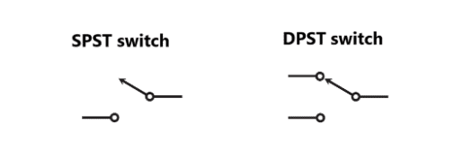
- Switch: The switch symbol represents making and breaking circuit connections within a circuit, making this symbol universally applicable.
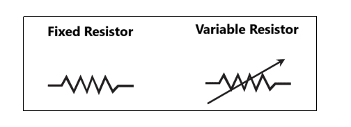
- Resistor: A resistor is an obstacle to current flow, hence drawn in a zigzag pattern. A variable resistor, on the other hand, can take desired values within a specific range, represented as a resistor with an arrow through the middle according to its symbol.
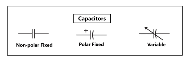
- Capacitor: A capacitor is used to store electrical energy in the form of charge. A capacitor internally has two plates for storing charge, so its symbol consists of two parallel lines spaced apart. Variable capacitors also exist, similar to resistors, with an arrow through the middle. Capacitors can be categorized as polar (having positive and negative polarity) and non-polar (having no polarity).
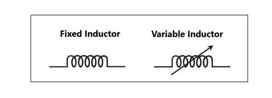
- Inductor: An inductor is also a device that stores energy in the form of a magnetic field. It is a non-polar device with a coil-like structure, hence its symbol is represented as:
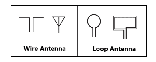
- Antenna: The antenna is the most commonly used device in RF electronics and is the first part of a receiver. An antenna transmits/receives electromagnetic waves, and its design may vary by application, but its symbol is as follows:
Power Supply Symbols:
- Battery: It is a source of energy composed of cells, containing chemical electrolyte internally that provides polarity. The cells in the battery symbol are represented by two parallel lines of unequal length, with the positive and negative terminals marked on them.
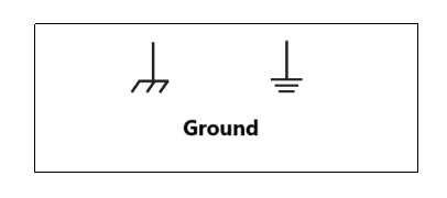
- Ground: Ground in an electrical network is the common reference point for voltage levels, providing a return path for current. It uses the symbol of the same name, represented as:
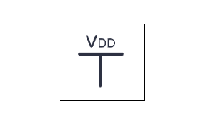
- VDD: In electrical networks, VDD represents the positive supply voltage for the circuit, typically used alongside the ground reference (GND). VDD and GND are label types connected to the battery, positive (VDD) and negative (GND) respectively. The symbol definition for VDD is as follows:
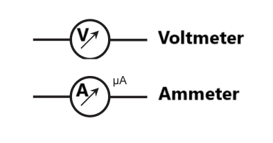
- Ammeter and Voltmeter: An ammeter measures current in an electrical network and is connected in series with circuit components. A voltmeter measures voltage across a component and is connected in parallel with circuit components. Both meters were traditionally analog, featuring moving coils, and their symbols are:
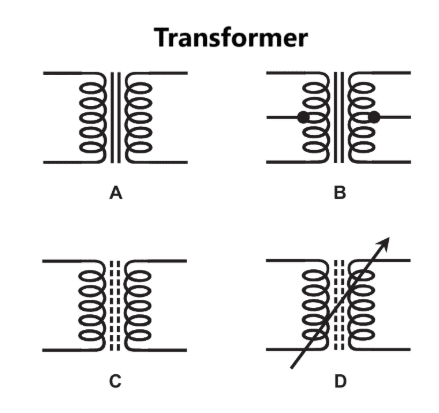
- Transformer: A transformer in an electrical network transfers electrical energy between circuits via electromagnetic induction. It consists of primary and secondary windings around a core, hence its symbol is represented as:
Active Analog/Digital Components:
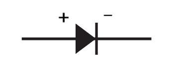
- Diode: In an electrical network, a diode acts like a one-way valve, allowing current to flow in only one direction. They are used for rectification (converting AC to DC) and protecting circuits by blocking reverse voltage. A diode is a polar device made from a PN junction, and its symbol is:
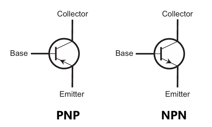
- Bipolar Junction Transistor (BJT): A transistor in an electronic network acts as a switch or amplifier for electrical signals. It is a three-terminal device that controls current between the collector and emitter terminals based on the voltage applied to the base terminal. BJTs come in two types, NPN (current sinking) and PNP (current sourcing), and the symbol represents the current sourcing/sinking type:
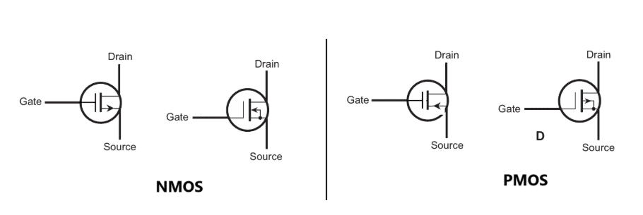
- MOSFET: A MOSFET is an improved transistor that operates on the same principle as a BJT. It is a three-terminal device that controls current between the drain and source based on the voltage applied to the gate. MOSFET stands for Metal-Oxide-Semiconductor Field-Effect Transistor; the metal oxide is an insulator material, making the gate resemble a capacitor, hence its symbol:
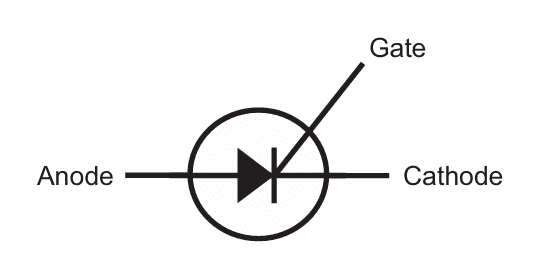
- SCR: An SCR (Silicon Controlled Rectifier) in an electronic network is a type of thyristor used for controlling high power. It acts as a switch, allowing current to flow when a gate signal is applied, and remains on until the current drops below a threshold. SCRs are used in power control and rectification. Its behavior is very similar to a diode with the gate terminal as an enable pin, hence the symbol:
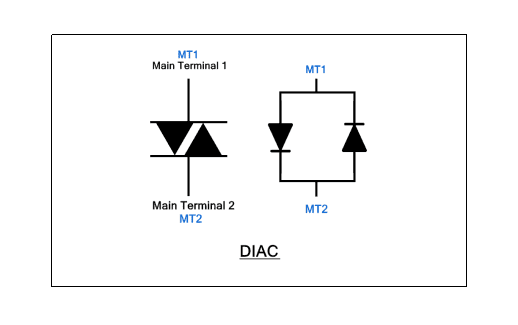
- DIAC: A DIAC (Diode for Alternating Current) in an electronic network is a bidirectional trigger device that conducts current only after its breakdown voltage is exceeded. Due to its bidirectional nature, its symbol is:
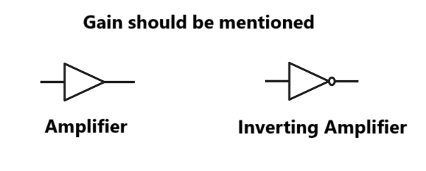
- Amplifier: An amplifier in an electronic network increases the power, voltage, or current of a signal. They are essential in audio, radio, and communication systems for boosting weak signals for transmission. Amplifiers may have different input and output terminals, and their standard symbol is:
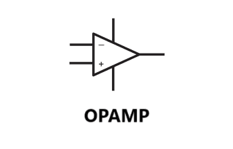
- Operational Amplifier (Op-Amp): An Operational Amplifier (Op-Amp) in an electronic network is a versatile, high-gain voltage amplifier with differential inputs. It is used in signal processing, filtering, and mathematical operations like addition, subtraction, integration, and differentiation. It is also a multi-pin device, and its symbol is:
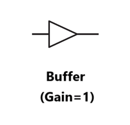
- Buffer: A buffer in an electronic network is used to isolate different stages of a circuit and prevent loading effects, which is crucial for maintaining signal integrity in complex circuits. It can be thought of as an amplifier with a gain of 1, so the input signal is reproduced at the output without any loss. The symbol for a buffer is:
Logic Gates:
Logic gates are fundamental building blocks of digital electronics, performing basic logical functions essential for circuit design and digital computation. They operate on binary inputs and produce a binary output based on a logic operation.
Types of Logic Gates:
- AND Gate: Outputs true (1) only if all inputs are true.
- OR Gate: Outputs true if at least one input is true.
- NOT Gate: Inverts the input; outputs true if the input is false.
- NAND Gate: Outputs false only if all inputs are true; otherwise outputs true.
- NOR Gate: Outputs true only if all inputs are false.
- XOR Gate: Outputs true if an odd number of inputs are true.
These gates are used in various combinations to perform complex logical operations and are integral to digital circuits, including computers and other electronic devices.
How to Create Symbols for Custom PCB Design
Transferring a circuit design to a Printed Circuit Board (PCB) is a multi-step process. First, the circuit schematic is created using suitable PCB design software. A schematic is essentially a circuit diagram containing various symbols, interconnected by wires as described previously. Then, using the same software, the schematic is converted into a PCB layout. The layout describes how the components are placed and routed on the physical PCB. To design a custom symbol, a part symbol file must be generated before schematic and layout design. A part symbol is simply a set of files containing all the electronic and geometric information of a component.
Here are the detailed steps for making your own symbol in a PCB design editor:
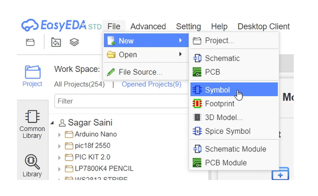
(The process is generally the same for most design software; here we use EasyEDA as an example. Please follow the instructions below.)
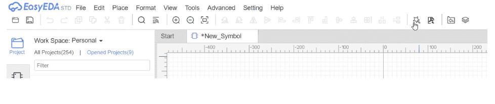
Step 1: Log in to EasyEDA and open the symbol design window. Navigate from the top menu to File -> New -> Symbol. A new blank schematic drawing window will open. Save it to your hard drive before proceeding. It’s recommended to name the file corresponding to the part name for which you are creating the symbol.
Step 2: Open the datasheet and review the pin information for the component you are designing within this window. Below is an example for the NE555 timer IC.
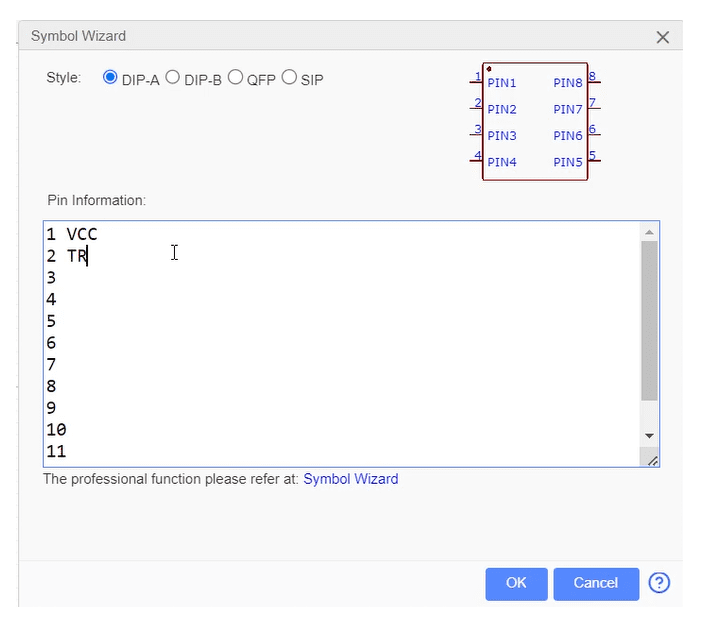
Step 3: EasyEDA provides a Symbol Wizard with some pre-defined built-in symbols for you to choose and use. Simply select the appropriate symbol and name all pins according to the symbol in the datasheet. This is an automatic symbol generator. If you wish to proceed manually, follow the steps below.
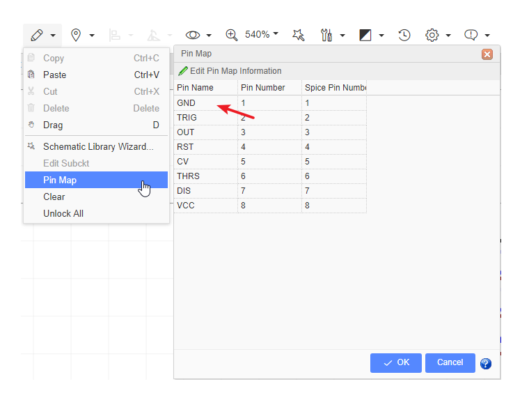
Pin information can be edited from:
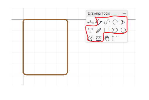
Step 4: To design the symbol manually, use the utilities in the drawing menu to draw the outline of the part’s top view. While most electronic chips are rectangular, you can actually draw any shape. The actual shape and size of the part are only important for the layout symbol, which will be created later.
Step 5: Open the pinout diagram from the component datasheet. This diagram shows the pins around the periphery of the component, with each pin labeled with its name nearby. Using the pin drawing utility, usually available in the left menu bar, draw the first pin at one corner of the component outline you drew earlier. Repeat this process for all component pins. A good practice is to try to replicate the pinout given in the component datasheet.
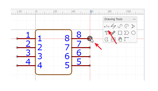
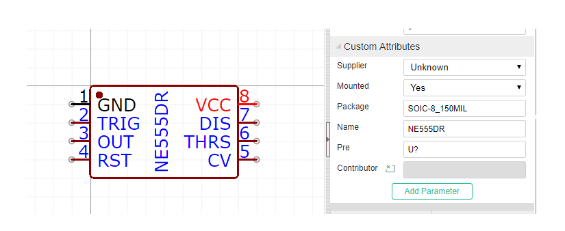
Step 6: Double-click on the first pin. A dialog box will open with details for that pin. Please enter its name from the component datasheet, e.g., VCC. Repeat this for all pins.
Step 7: Modify all other pin details as needed.
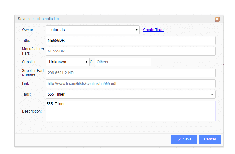
Step 8: Enter all required details and save the file. Your PCB component symbol is now created.
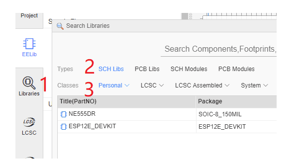
Step 9: Browse the component library and double-click on the layout symbol you saved earlier. This will open the symbol in the layout view.
Conclusion
Circuit symbols are indispensable tools for understanding, designing, and troubleshooting electrical and electronic circuits. By utilizing standardized symbols, engineers and technicians ensure accurate communication, reduce errors, and streamline the design process. Understanding the importance and usage of circuit symbols empowers professionals to work with and manage electrical and electronic systems effectively.


0 Comments