
Leveraging our global technical team, we possess a comprehensive understanding of the requirements and manufacturing methods necessary for successful HDI products. Learn more about HDI PCB technical specifications, how IPC defines HDI boards, and some design tips.
What is an HDI PCB Microcircuit?
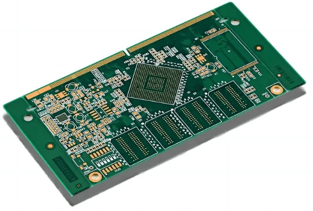
A High-Density Interconnect Printed Circuit Board (HDI PCB) is a type of circuit board that offers a higher wiring density per unit area compared to traditional boards. This enables more components to be accommodated within the total available space. HDI PCBs contribute to enhanced electrical performance while reducing the weight and size of devices.
HDI PCBs feature smaller vias and pads, finer pitch and traces, and a higher connection pad density, making them a superior choice for space-constrained boards. HDI technology is commonly used in products like mobile phones, personal computers, MP3 players, gaming consoles, and more.
What is the Definition of an HDI Board?
IPC-2226 defines HDI as a printed circuit board with a wiring density per unit area higher than that of traditional printed circuit boards (PCBs). Compared to conventional PCB technology, HDI boasts finer trace widths and spacing (≤ 100 µm / 0.10mm), smaller vias (<150 µm), and smaller pads (<400 µm / 0.40mm), along with a higher connection pad density (>20 pads/cm²). HDI characteristics are categorized into Type I, Type II, and Type III.
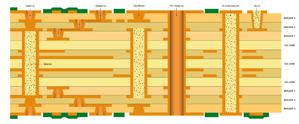
Different Types of HDI Characteristics
The diagram below shows the primary structures defined in IPC-2226 – Type I, Type II, and Type III.
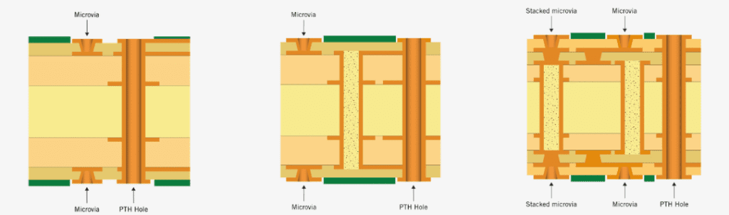
- Type I. Refers to a single microvia layer on one or both sides of the core. Uses plated microvias and PTHs for interconnection, employing blind vias rather than buried vias.
- Type II. Refers to one microvia layer on each of one or both sides of the core. Uses plated microvias and through-vias (PTH) for interconnection. Employs both blind and buried vias.
- Type III. Refers to at least two layers of microvias on one or both sides of the core. Uses plated microvias and through-vias (PTH) for interconnection. Employs both blind and buried vias.
Architectural Terms Defining HDI Construction Degree:
1+n+1= Single layer of microvias (per Type I and II examples above)2+n+2= 2 layers of microvias (per Type III example above)3+n+3= 3 layers of microvias
Differences Between HDI PCBs and Standard PCBs
HDI boards differ significantly from standard PCB boards in structure, process, and application. Standard PCBs primarily use FR-4 epoxy material, rely mainly on mechanically drilled through-holes, and typically have trace width/spacing ≥100μm.
HDI boards use laser drilling to form microvias (aperture <150μm), employ blind and buried via designs, and can have trace width/spacing less than 50μm. The multilayer structure of HDI boards (usually 8 layers or more) achieves any-layer interconnection through laser drilling and stacked via technology, whereas standard PCBs are mostly simple laminates, typically with ≤8 layers.
Regarding materials, HDI boards use high-performance materials like polyimide and low-dielectric constant materials, while standard PCBs use ordinary FR-4 epoxy resin, etc. These differences allow HDI boards far exceed standard PCBs in density, performance, and applicability.
Technical Features and Core Advantages of HDI PCBs
The core of HDI PCBs lies in their high-density interconnect technology, primarily achieved through microvia technology, blind/buried vias, and any-layer interconnects. Microvia technology uses laser drilling to form tiny holes (e.g., 0.1mm diameter), offering higher precision and smaller apertures compared to mechanical drilling in standard PCBs.
Blind and buried via technology reduces space occupation through non-through holes, increasing wiring density. Any-layer interconnect (Any-layer HDI) enables direct connection between any two layers in high-end HDI boards, allowing for more flexible routing.
Advantages of HDI boards include: smaller volume, suitable for portable devices; faster signal transmission (reduced parasitic effects); support for high-pin-count chips (e.g., BGA packaging); improved signal integrity and reliability; and enhanced thermal performance and electromagnetic compatibility.
These advantages make HDI boards indispensable in high-end electronic devices, providing greater design flexibility and higher performance.
Routing Guidelines in HDI PCB Design
Common Routing Guidelines for HDI Board Layouts
As component density increases, routing on HDI boards becomes highly complex. To accommodate high-density routing in HDI PCB designs, trace width, via size, and spacing must be minimized. In HDI PCB design, all critical signal components, decoupling capacitors, and ICs must be routed first, followed by complete routing of the remaining components.
Best practice involves creating multilayer boards and using ground and power planes as inner layers to minimize noise and crosstalk caused by high-speed signals. These ground and power planes are placed such that a ground plane is directly beneath a signal layer, acting as a return path and reference layer for top-layer differential signals. The power plane is placed after the ground plane to reduce impedance.
To provide a separate ground plane for each signal, the split-plane concept must be used for copper pouring. This avoids noise from different signals and components, enabling better performance in HDI PCB design without interference from adjacent signals.
Other Guidelines for HDI Board Routing
Furthermore, when routing differential pair signals, they must be routed symmetrically, maintaining a specified distance between them to achieve the designated impedance. Improper routing of these pairs can cause signal delay at the receiving end. There should be no components or vias between these signals. Placing components or vias between them can lead to EMI/EMC issues and impedance mismatch in the HDI PCB design.
Additionally, differential pairs require very tight delay matching between the positive and negative signals. To achieve this tight delay matching, length tuning using serpentine geometries must be employed in the HDI PCB design.
Component Placement in HDI PCB Design
Component placement plays a crucial role in HDI PCB (High-Density PCB Design) design, as it directly affects the board’s routing density and signal integrity. Planning component placement is essential for maintaining the shortest paths. Always group components according to the schematic workflow, separate sensitive and critical components, and place them accordingly.
As an initial step, read the schematic and divide the circuit into different sections based on: analog, digital, high-speed signals, mixed signals and high frequency, power, etc.
After grouping the components, place the main components (such as microprocessors or microcontrollers, Ethernet, and memory devices) in the central area of the board, as they connect to most components in the circuit. Next, place all decoupling capacitors, crystal oscillators, and resistors as close as possible to these components to ensure smooth signal transfer between them.
Some key considerations for component placement are as follows:
- Component Orientation in HDI PCB Design: Components must be placed in the same orientation to enable efficient and error-free routing during the HDI PCB design process and an error-free soldering process during assembly.
- Placement Side for Components: All SMD components should be placed on the same side, either top or bottom. All through-hole components should be placed on the top to simplify the assembly process.
- Separating Analog and Digital Circuit Sections: Separate analog and digital sections to avoid noise interference from each other.
- Placement of Decoupling and Bypass Capacitors: Place all decoupling and bypass capacitors as close as possible to their respective circuit sections.
- Placement of Sensitive Components: Place all sensitive components away from the board edges to reduce the impact of EMI radiated from peripherals.
Now, place all peripherals at the edges of the board for communication with external devices.
Application Areas of HDI PCBs
Smartphones and Consumer Electronics
Smartphones are one of the most important application areas for HDI boards. For example, the iPhone 6 motherboard used 5th-order HDI technology. HDI boards make consumer electronics like smartphones, tablets, and wearables thinner and lighter while providing powerful functionality and long battery life.
Communication Equipment
In communication equipment such as 5G base stations, routers, and switches, HDI boards provide higher signal integrity and lower latency, supporting high-speed data transmission and complex signal processing. With the proliferation of 5G technology, the application of HDI boards in the communication field will further expand.
Computers and Servers
High-performance computing, data centers, and cloud computing equipment widely use HDI boards (e.g., 10-layer 3rd-order HDI PCBs), enabling higher data processing speeds and greater storage capacity to meet the demands of the big data era. The rise of AI servers has further driven the application of high-layer-count HDI boards and ultra-low-loss materials.
Automotive Electronics
With the development of electric vehicles and autonomous driving technology, the performance requirements for automotive electronics are increasing. HDI boards can meet these requirements, providing a stable operating environment for automotive electronic systems.
Aerospace and Defense
These fields have extremely high requirements for the reliability and performance of electronic equipment. The application of HDI boards improves system stability, enhances anti-interference capability, and ensures the successful completion of critical missions.
HDI PCB Design Tips
Nothing influences the cost and quality of a PCB more than the initial design. Here you can find practical information about common design issues, the production problems they can cause, and most importantly—the best solutions to avoid them!
| Common HDI Design Issue | Production Problem Depends On This | Best Solution |
|---|---|---|
| Dielectric too thick for laser via | – Increased laser drilling time, reduced productivity. – High risk of voids during plating, especially at microvia bottom. – Increased PCB price due to lower yield. | Use an aspect ratio below 0.8:1. |
| Microvia size too small | – Increased risk of microvias being blocked by unknown material, preventing satisfactory plating. – High risk of poor microvia plating, especially at the bottom. – Increased PCB price due to lower yield. | – For microvias intended for copper filling, use 100 μm microvias with an aspect ratio below 0.8:1. – For microvias not requiring copper filling, use 125 μm microvias with an aspect ratio below 0.8:1. |
| Capture and target pads for microvias too small, geometry too tight | – If target pad is too small, risk of partial missing (so-called over-shoot) increases, and material near the pad will be burned down to the next layer. – If capture pad is too small, risk of pad fracture exists, which is unacceptable for any class in IPC-6016. | If possible, use a starting pad 200 μm larger than the microvia. For tighter geometries, consult NCAB. |
| Pit requirements for copper-filled microvias too strict | Increased PCB price due to lower yield. | Set pit requirement to a maximum of 25 μm. |
| Overly strict plating thickness requirements for plugged through-vias. (POFV or VIPPO) | Affects process flow. With reasonable plating thickness, all vias can be done in the same operation, greatly simplifying the process. Excessively thick plating reduces possibility of fine outer layer traces/isolations. | Set requirements according to IPC-6012 Class II standard, requiring only over-plating thickness ≥6μm. |
| Epoxy plugging requires too many different via sizes, applies to buried vias and through-vias | Difficult to control final plugging without air bubbles and ensure complete filling is problem-free. | Recommend using only one size of plugged via; if more sizes must be plugged, keep them within a 0.15 mm range. |
| Microvia Placement | If microvias are placed directly under SMD pads, unwanted voids may appear in the solder joint during reflow soldering. If microvias are copper-filled, the price will be higher. | If possible, pull microvias back from SMD pads. If no space for option 1, place microvia directly in the pad and request copper filling. |
| Distance between staggered vias too small – microvia to microvia or microvia to buried via | If staggered microvias are too close, risk exists that upper microvia may intrude into lower microvia, causing poor plating. This can be solved by copper filling in the lower microvia or over-plating the buried via, but this increases cost and risk. | For microvia to microvia, keep hole-to-hole distance 0.30 mm if possible; if not enough, reduce to 0.25 mm. E.g., 0.10mm microvia and 0.25mm buried via, center distances 0.475mm and 0.425mm respectively. |
HDI PCB Design Guidelines
Minimum Track and Gap for Tent & Plate
IPC-4761 Type VII Via-in-Pad Plated Over / VIPPO / POFV
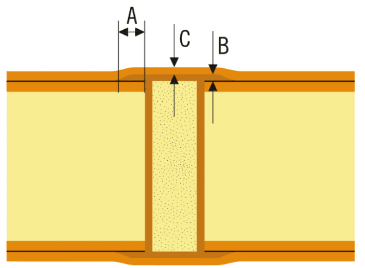
A. Minimum copper tenting overhang 25 μm for Class 1, 2, and 3
B. Minimum copper tenting thickness 5 μm for Class 2 and 3
C. Minimum cap plating 12 μm for Class 3, 5 μm for Class 2
HDI PCBs: Making the Right Choices from Design to Production
wo key factors for successful HDI PCB production are: first, making the right choices during the design phase, and then carefully selecting a manufacturer capable of supporting the project’s specific technical needs.
Whether in consumer electronics, computers, automotive, or medical technology, the overall trend is miniaturization. This is evident not only in the reduction of physical size or finished product dimensions but also because components themselves are becoming smaller and must be packed more densely using finer features.
As electronics become more complex, more advanced PCBs are becoming increasingly common. These specifications demand High-Density Interconnect (HDI) solutions with higher layer counts, more connections on and within the PCB surface, and utilization of finer conductor widths and narrower conductor spacing.
Increased layer counts and microvia technology also require the use of thinner prepregs and core laminates than traditionally manufactured boards, placing higher demands on the manufacturer.
Balancing Cost and Reliability
The manufacturing of HDI boards requires finding a balance between cost and reliability. When using any layer interconnect design, the cost increases by about 15% -20% and the yield decreases for each additional layer added.
In mass production, engineers often prefer to choose staggered stacking structures (such as 1+N+1) to ensure the majority of high-density requirements while keeping costs within a reasonable range.
Another misconception is blindly pursuing the minimization of line width/spacing. For example, reducing the line width from 40 μ m to 30 μ m can increase the wiring space by 10%, but it will lead to an increase in etching accuracy requirements, a decrease in yield (from over 95% to 85%), and an increase in impedance control difficulty.
In practical design, it is usually recommended to use limit parameters only in critical areas such as RF wiring, while leaving a certain margin for general signal lines.
Future Development Trends
With the gradual recovery of the global economy, rebounding demand in end markets like mobile phones, automotive electronics, and laptops, coupled with strong demand from AI servers and satellite communications, HDI became the PCB product with the highest global growth rate in 2025, a momentum expected to continue into 2026.
Technologically, HDI PCBs are advancing towards higher density, finer lines, and lower loss. The rapid rise of the AI server market not only drives growth in high-end application demand but also, due to its high-unit-price characteristic, opens a new development path for HDI technology, moving towards high-layer-count stack-ups and ultra-low-loss materials.
The application of laser drilling, nano-level materials, and smart manufacturing technologies will become industry priorities, helping achieve higher performance and smaller electronic products. Any-layer HDI technology will also see wider application, further reducing PCB volume and increasing wiring density.
Summary
With the rapid development of 5G, AI, and the Internet of Things (IoT), HDI PCB technology is moving towards higher density, finer lines, and lower loss.
The application of laser drilling, nano-level materials, and smart manufacturing technologies will become industry focal points, aiding in the realization of higher-performance, smaller-volume electronic products. The global HDI market is projected to be the highest-growing PCB product in 2024, continuing into 2025.
From smartphones to aerospace, from consumer electronics to defense, HDI PCB technology has become an indispensable foundation for modern electronic equipment.


0 Comments