



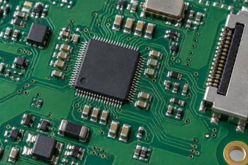
5G communication PCB
High-Speed PCB Layout Guidelines: Timing and Return Paths
Good high-speed PCB layout starts with the signal’s edge rate, an agreed stackup and a continuous return path. Then turn the interface requirements into routing constraints, check electrical delay rather than length alone, and verify the complete connection through vias and connectors before releasing fabrication files. A clock frequency by Read more