Blog
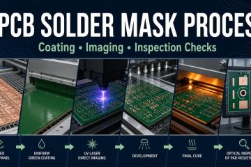
PCB Solder Mask Process: Coating, Imaging and Inspection Checks
See how PCB solder mask is prepared, coated, imaged, developed, cured and inspected for registration, coverage and adhesion defects.




See how PCB solder mask is prepared, coated, imaged, developed, cured and inspected for registration, coverage and adhesion defects.
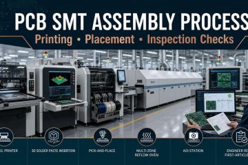
Follow PCB SMT assembly from file and material control through paste printing, SPI, placement, reflow, AOI, X-ray and electrical test.
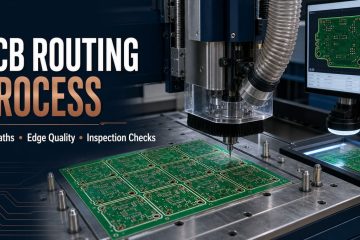
See how PCB CNC routing controls profile data, toolpaths, fixtures, tabs, edge quality, depaneling and dimensional inspection.
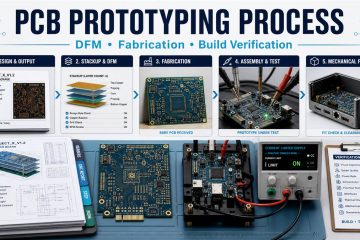
Follow the PCB prototyping process from design objectives and DFM through fabrication, assembly, bring-up, verification and revision release.
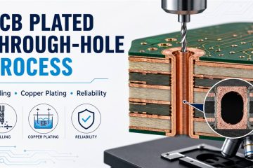
See how plated through holes are drilled, desmeared, activated and copper plated, plus the controls, defects and tests that determine PTH reliability.
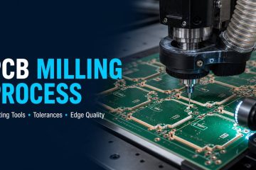
Learn how PCB milling controls routing data, cutter selection, compensation, feeds, tool wear, edge tolerances, burrs and finished-board inspection.
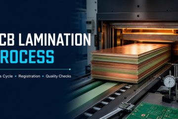
Learn how multilayer PCB lamination controls prepreg, resin flow, vacuum, temperature, pressure, registration, thickness, voids and delamination.
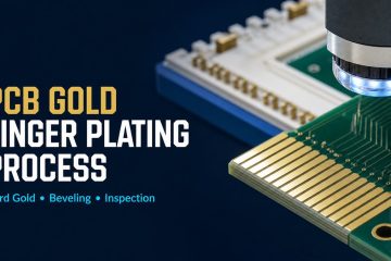
Learn how PCB gold fingers are selectively hard-gold plated over nickel, then beveled and inspected for thickness, adhesion, wear and connector fit.
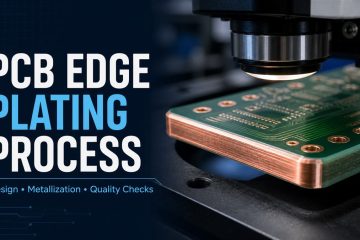
Learn how PCB edge plating is designed and manufactured, including wrap copper, profile preparation, metallization, finishes, defects and inspection.
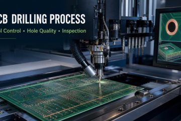
See how PCB drilling uses mechanical and laser processes, with controls for registration, tool wear, smear, hole quality, plating and inspection.
If you have any enquiry about quotation or cooperation, please feel free to email us at sales@pcbtry.com or use the following enquiry form. Oursales representative will contact you within 24 hours. Thank you for your interest in our products.